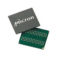
MT46H16M32LFCM-6 IT:B Micron Technology Inc, MT46H16M32LFCM-6 IT:B Datasheet - Page 89

MT46H16M32LFCM-6 IT:B
Manufacturer Part Number
MT46H16M32LFCM-6 IT:B
Description
Manufacturer
Micron Technology Inc
Type
DDR SDRAMr
Datasheet
1.MT46H16M32LFCM-6_ITB.pdf
(98 pages)
Specifications of MT46H16M32LFCM-6 IT:B
Organization
16Mx32
Density
512Mb
Address Bus
15b
Access Time (max)
6.5/5ns
Maximum Clock Rate
166MHz
Operating Supply Voltage (typ)
1.8V
Package Type
VFBGA
Operating Temp Range
-40C to 85C
Operating Supply Voltage (max)
1.95V
Operating Supply Voltage (min)
1.7V
Supply Current
115mA
Pin Count
90
Mounting
Surface Mount
Operating Temperature Classification
Industrial
Lead Free Status / Rohs Status
Compliant
AUTO REFRESH Operation
Figure 49: Auto Refresh Mode
PDF: 09005aef82d5d305
512mb_ddr_mobile_sdram_t47m.pdf – Rev. I 12/09 EN
Command
BA0, BA1
Address
DQS
DM
CKE
DQ
CK#
A10
CK
6
6
1
6
t
t
IS
IS
NOP 2
T0
t
t
IH
IH
Notes:
Bank(s)
One bank
All banks
PRE
T1
Auto refresh mode is used during normal operation of the device and is analogous to
CAS#-BEFORE-RAS# (CBR) REFRESH in FPM/EDO DRAM. The AUTO REFRESH com-
mand is nonpersistent and must be issued each time a refresh is required.
The addressing is generated by the internal refresh controller. This makes the address
bits a “Don’t Care” during an AUTO REFRESH command.
For improved efficiency in scheduling and switching between tasks, some flexibility in
the absolute refresh interval is provided. The auto refresh period begins when the AU-
TO REFRESH command is registered and ends
Although it is not a JEDEC requirement, CKE must be active (HIGH) during the auto
refresh period to provide support for future functional features. The auto refresh period
begins when the AUTO REFRESH command is registered and ends
5
1. PRE = PRECHARGE; AR = AUTO REFRESH.
2. NOP commands are shown for ease of illustration; other commands may be valid during
3. NOP or COMMAND INHIBIT are the only commands supported until after
4. The second AUTO REFRESH is not required and is only shown as an example of two back-
5. Bank x at T1 is “Don’t Care” if A10 is HIGH at this point; A10 must be HIGH if more than
6. DM, DQ, and DQS signals are all “Don’t Care”/High-Z for operations shown.
t
CK
this time. CKE must be active during clock positive transitions.
must be active during clock positive transitions.
to-back AUTO REFRESH commands.
one bank is active (for example, must precharge all active banks).
NOP
Valid
T2
2
t
CH
t
RP
t
CL
NOP
T3
2
89
T4
AR
(
(
(
(
512Mb: x16, x32 Mobile LPDDR SDRAM
(
(
(
(
(
(
(
)
)
)
(
)
(
(
)
)
(
)
(
)
(
)
(
)
)
)
)
)
)
) )
) )
)
)
)
(
(
(
(
(
(
(
(
(
(
(
)
(
(
)
)
(
)
(
)
)
)
(
)
(
)
(
)
)
)
)
)
)
)
)
)
NOP
t
Ta0
RFC
Micron Technology, Inc. reserves the right to change products or specifications without notice.
2, 3
t
RFC later.
Ta1
AR
4
AUTO REFRESH Operation
(
(
(
(
( (
(
(
(
(
(
(
)
)
(
) )
(
)
(
(
)
)
(
)
(
)
(
)
(
)
)
)
)
) )
)
)
)
)
)
)
(
(
(
(
(
(
(
(
(
)
)
(
)
)
(
(
(
(
)
)
(
(
)
(
)
(
)
)
)
)
)
)
)
)
)
)
NOP
Valid
Tb0
2, 3
© 2004 Micron Technology, Inc. All rights reserved.
t
RFC
4
t
RFC later.
NOP 2
Tb1
t
RFC time; CKE
Don’t Care
ACTIVE
Bank
Tb2
Row
Row


