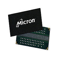
MT47H32M16HR-25E IT:F TR Micron Technology Inc, MT47H32M16HR-25E IT:F TR Datasheet - Page 111

MT47H32M16HR-25E IT:F TR
Manufacturer Part Number
MT47H32M16HR-25E IT:F TR
Description
Manufacturer
Micron Technology Inc
Type
DDR2 SDRAMr
Datasheet
1.MT47H32M16HR-25E_ITF_TR.pdf
(131 pages)
Specifications of MT47H32M16HR-25E IT:F TR
Organization
32Mx16
Density
512Mb
Address Bus
15b
Access Time (max)
400ps
Maximum Clock Rate
800MHz
Operating Supply Voltage (typ)
1.8V
Package Type
FBGA
Operating Temp Range
-40C to 85C
Operating Supply Voltage (max)
1.9V
Operating Supply Voltage (min)
1.7V
Supply Current
295mA
Pin Count
84
Mounting
Surface Mount
Operating Temperature Classification
Industrial
Lead Free Status / Rohs Status
Compliant
- Current page: 111 of 131
- Download datasheet (10Mb)
Figure 65: Data Input Timing
PRECHARGE
PDF: 09005aef82f1e6e2
512MbDDR2.pdf - Rev. Q 10/10 EN
Notes:
DQS#
Precharge can be initiated by either a manual PRECHARGE command or by an autopre-
charge in conjunction with either a READ or WRITE command. Precharge will deacti-
vate the open row in a particular bank or the open row in all banks. The PRECHARGE
operation is shown in the previous READ and WRITE operation sections.
During a manual PRECHARGE command, the A10 input determines whether one or all
banks are to be precharged. In the case where only one bank is to be precharged, bank
address inputs determine the bank to be precharged. When all banks are to be pre-
charged, the bank address inputs are treated as “Don’t Care.”
Once a bank has been precharged, it is in the idle state and must be activated prior to
any READ or WRITE commands being issued to that bank. When a single-bank PRE-
CHARGE command is issued,
mand is issued,
DQS
CK#
DM
DQ
CK
1.
2.
3. Subsequent rising DQS signals must align to the clock within
4. WRITE command issued at T0.
5. For x16, LDQS controls the lower byte and UDQS controls the upper byte.
6. WRITE command with WL = 2 (CL = 3, AL = 0) issued at T0.
t
t
DSH (MIN) generally occurs during
DSS (MIN) generally occurs during
T0
WL - t DQSS (NOM)
t
RPA timing applies, regardless of the number of banks opened.
T1
T1n
t WPRE
111
t
T2
DI
RP timing applies. When the PRECHARGE (ALL) com-
t DSH 1
T2n
t DQSL
t DSS 2
t
t
DQSS (MAX).
DQSS (MIN).
Micron Technology, Inc. reserves the right to change products or specifications without notice.
Transitioning Data
T3
3
t DQSH
512Mb: x4, x8, x16 DDR2 SDRAM
t DSH 1
T3n
t WPST
t DSS 2
T4
Don’t Care
© 2004 Micron Technology, Inc. All rights reserved.
t
DQSS.
PRECHARGE
Related parts for MT47H32M16HR-25E IT:F TR
Image
Part Number
Description
Manufacturer
Datasheet
Request
R

Part Number:
Description:
IC DDR2 SDRAM 512MBIT 84FBGA
Manufacturer:
Micron Technology Inc
Datasheet:

Part Number:
Description:
IC DDR2 SDRAM 512MBIT 3NS 84FBGA
Manufacturer:
Micron Technology Inc
Datasheet:

Part Number:
Description:
32MX16 DDR2 SDRAM PLASTIC IND TEMP PBF FBGA 1.8V
Manufacturer:
Micron Technology Inc
Datasheet:

Part Number:
Description:
DRAM Chip DDR2 SDRAM 512M-Bit 32Mx16 1.8V 84-Pin FBGA T/R
Manufacturer:
Micron Technology Inc
Datasheet:

Part Number:
Description:
Manufacturer:
Micron Technology Inc
Datasheet:

Part Number:
Description:
Manufacturer:
Micron Technology Inc
Datasheet:

Part Number:
Description:
Manufacturer:
Micron Technology Inc
Datasheet:

Part Number:
Description:
Manufacturer:
Micron Technology Inc
Datasheet:

Part Number:
Description:
MICMT47H32M16HR-3_IT:F 32MBX16 DDR2
Manufacturer:
Micron Technology Inc
Datasheet:

Part Number:
Description:
Manufacturer:
Micron Technology Inc
Datasheet:

Part Number:
Description:
Manufacturer:
Micron Technology Inc
Datasheet:

Part Number:
Description:
32MX16 DDR2 SDRAM PLASTIC IND TEMP PBF FBGA 1.8V
Manufacturer:
Micron Technology Inc

Part Number:
Description:
IC DDR2 SDRAM 512MBIT 84FBGA
Manufacturer:
Micron Technology Inc
Datasheet:

Part Number:
Description:
Manufacturer:
Micron Technology Inc
Datasheet:

Part Number:
Description:
Manufacturer:
Micron Technology Inc
Datasheet:


