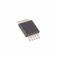
MAX5741EUB+T Maxim Integrated Products, MAX5741EUB+T Datasheet

MAX5741EUB+T
Specifications of MAX5741EUB+T
Related parts for MAX5741EUB+T
MAX5741EUB+T Summary of contents
Page 1
... Power Amplifier Control Process Control I/O Boards Battery-Powered Instruments VCO Control Functional Diagram appears at end of data sheet. µMAX is a registered trademark of Maxim Integrated Products, Inc. SPI and QSPI are trademarks of Motorola, Inc. MICROWIRE is a trademark of National Semiconductor, Corp. ________________________________________________________________ Maxim Integrated Products For pricing, delivery, and ordering information, please contact Maxim Direct at 1-888-629-4642, or visit Maxim’ ...
Page 2
Low-Power, Quad, Voltage-Output DAC with Serial Interface ABSOLUTE MAXIMUM RATINGS V to GND ..............................................................-0.3V to +6V DD OUT_, SCLK, DIN, CS, REF to GND...............-0 Maximum Continuous Current Into Any Pin......................±50mA Continuous Power Dissipation (T = +70°C) A ...
Page 3
Low-Power, Quad, Voltage-Output ELECTRICAL CHARACTERISTICS (continued +2.7V to +5.5V, GND = REF V = +5V +25°C PARAMETER SYMBOL DIGITAL INPUTS (SCLK, DIN, CS) Input High Voltage Input Low Voltage Input ...
Page 4
Low-Power, Quad, Voltage-Output DAC with Serial Interface __________________________________________Typical Operating Characteristics ( +25°C, unless otherwise noted.) REF DD A INTEGRAL NONLINEARITY vs. CODE +25° + ...
Page 5
Low-Power, Quad, Voltage-Output ( +25°C, unless otherwise noted.) REF DD A WORST-CASE INL AND DNL vs. TEMPERATURE MAXIMUM DNL MAXIMUM INL MINIMUM DNL MINIMUM INL - ...
Page 6
Low-Power, Quad, Voltage-Output DAC with Serial Interface ( +25°C, unless otherwise noted.) REF DD A FULL-SCALE SETTLING TIME (V CODE 000 TO 3FF HEX 1µs/div HALF-SCALE SETTLING TIME (V CODE ...
Page 7
Low-Power, Quad, Voltage-Output ( +25°C, unless otherwise noted.) REF DD A DIGITAL-TO-ANALOG GLITCH IMPULSE (V = +3V) DD 1µs/div DIGITAL-TO-ANALOG GLITCH IMPULSE (V = +3V) DD 1µs/div POWER-ON RESET, SLOW RISE TIME (V = ...
Page 8
Low-Power, Quad, Voltage-Output DAC with Serial Interface (V = +3V +25°C, unless otherwise noted.) DD REF DD A POWER-ON RESET, SLOW RISE-TIME (V = +3V) DD 40µs/div CLOCK FEEDTHROUGH (V 2µs/div CODE 200 ...
Page 9
Low-Power, Quad, Voltage-Output PIN NAME CS 1 Chip-Select Input 2 SCLK Serial Clock Input 3 V Power-Supply Input DD 4 GND Ground 5 DIN Serial Data Input 6 REF External Reference Voltage Input DAC Voltage Outputs. Power-on reset sets ...
Page 10
Low-Power, Quad, Voltage-Output DAC with Serial Interface Table 1. Power-Down Mode Control EXTENDED CONTROL D9– ...
Page 11
Low-Power, Quad, Voltage-Output CONTENTS OF INPUT SHIFT D9 (MSB Figure 1. 16-Bit Input Word SCLK t CSW CS DIN Figure 2. Timing Diagram The digital inputs are compatible with CMOS logic. In order to ...
Page 12
Low-Power, Quad, Voltage-Output DAC with Serial Interface Table 2. Serial-Interface Programming Commands CONTROL DATA BITS D9– ...
Page 13
Low-Power, Quad, Voltage-Output Table 3. Unipolar Code Table DAC CONTENTS ANALOG OUTPUT 1111 1111 1100 1000 0000 0100 1000 0000 0000 0111 1111 1100 0000 0000 0100 0000 0000 0000 Chip Information TRANSISTOR COUNT: 14458 PROCESS: BiCMOS ______________________________________________________________________________________ DAC ...
Page 14
Low-Power, Quad, Voltage-Output DAC with Serial Interface V DD INPUT REGISTER A INPUT REGISTER B INPUT REGISTER C INPUT REGISTER D INPUT CONTROL LOGIC AND SHIFT REGISTER CS SCLK 14 ______________________________________________________________________________________ REF OUTPUT DAC 10-BIT DAC REGISTER A BUFFER ...
Page 15
... Maxim cannot assume responsibility for use of any circuitry other than circuitry entirely embodied in a Maxim product. No circuit patent licenses are implied. Maxim reserves the right to change the circuitry and specifications without notice at any time. Maxim Integrated Products, 120 San Gabriel Drive, Sunnyvale, CA 94086 408-737-7600 ____________________ 15 © 2008 Maxim Integrated Products ...


