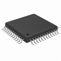
MAX5856AECM+TD Maxim Integrated Products, MAX5856AECM+TD Datasheet - Page 19

MAX5856AECM+TD
Manufacturer Part Number
MAX5856AECM+TD
Description
IC DAC 8BIT DUAL 300MSPS 48-TQFP
Manufacturer
Maxim Integrated Products
Datasheet
1.MAX5856AECMD.pdf
(23 pages)
Specifications of MAX5856AECM+TD
Settling Time
11ns
Number Of Bits
8
Data Interface
Parallel
Number Of Converters
2
Voltage Supply Source
Single Supply
Power Dissipation (max)
792mW
Operating Temperature
-40°C ~ 85°C
Mounting Type
Surface Mount
Package / Case
48-TQFP Exposed Pad, 48-eTQFP, 48-HTQFP, 48-VQFP
Lead Free Status / RoHS Status
Lead free / RoHS Compliant
Figure 6 illustrates the DAC write cycle in 4x interpola-
tion mode. With the interpolation feature enabled, the
device can operate with the PLL enabled or disabled.
To obtain best phase noise performance, disable the
PLL and keep the capacitive load at the CLK output low
(10pF or less at f
With the PLL disabled (PLLEN = 0), the clock signal is
applied to CLKXP/CLKXN and internally divided by 4 to
generate the DAC’s CLK signal. The CLK signal is a
divide-by-4 output, used to synchronize data into the
MAX5856A data ports. The CLKXP/CLKXN signal dri-
ves the interpolation filters and DAC cores at the
desired conversion rate.
If the PLL is enabled (PLLEN = 1), then CLK becomes
an input and the clock signal may be applied to CLK. In
Figure 6, the CLK signal is multiplied by a factor of four
by the PLL and distributed to the interpolation filters
and DAC cores. In this mode, CLKXP must be pulled
low and CLKXN pulled high.
Figure 6. Timing Diagram for Noninterleave Data Mode (IDE = Low)
CONTROL WORD
DA0–DA7/
DB0–DB7
CLKXN
CLKXP
CLK
CW
1. CLKXP AND CLKXN MUST BE PRESENT ONLY WHEN PLL IS DISABLED, WITH PLLEN CONNECTED TO GND. THE DIAGRAM SHOWS 4x INTERPOLATION.
2. CLK IS AN OUTPUT WHEN PLL IS DISABLED, WITH PLLEN CONNECTED TO GND; OTHERWISE, IT IS AN INPUT.
1
1
DAC
______________________________________________________________________________________
= 165MHz).
Dual 8-Bit, 300Msps DAC with 4x/2x/1x
t
DCSR
DA
DB
N
N
t
CXD
Interpolation Filters and PLL
t
CXD
The MAX5856A can operate with a single-ended clock
input used as both data clock and conversion clock. To
operate the device in this mode, disable the interpolation
filters and enable the PLL (PLLEN = 1). Apply a single-
ended clock input at CLK. The CLK signal acts as the
data synchronization clock and DAC core conversion
clock. Though the PLL is enabled, the lock pin (LOCK) is
not valid and the PLL is internally disconnected from the
interpolating filters and DAC cores. In this mode, CLKXP
must be pulled low and CLKXN pulled high.
Figure 6 shows the timing for the CW. An 8-bit control
word routed through channel A’s data port programs
the gain matching, interpolator configuration, and oper-
ational mode of the MAX5856A. The control word is
latched on the falling edge of CW. The CW signal is
asynchronous with conversion clocks CLK and
CLKXN/CLKXP; therefore, the conversion clock (CLK or
CLKXN/CLKXP) can run uninterrupted when a control
word is written to the device.
CONTROL WORD
t
CWH
t
CWS
DA
DB
N+1
N+1
t
DCHR
19


