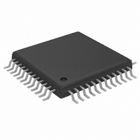
MAX5856AECM+TD Maxim Integrated Products, MAX5856AECM+TD Datasheet - Page 20

MAX5856AECM+TD
Manufacturer Part Number
MAX5856AECM+TD
Description
IC DAC 8BIT DUAL 300MSPS 48-TQFP
Manufacturer
Maxim Integrated Products
Datasheet
1.MAX5856AECMD.pdf
(23 pages)
Specifications of MAX5856AECM+TD
Settling Time
11ns
Number Of Bits
8
Data Interface
Parallel
Number Of Converters
2
Voltage Supply Source
Single Supply
Power Dissipation (max)
792mW
Operating Temperature
-40°C ~ 85°C
Mounting Type
Surface Mount
Package / Case
48-TQFP Exposed Pad, 48-eTQFP, 48-HTQFP, 48-VQFP
Lead Free Status / RoHS Status
Lead free / RoHS Compliant
The MAX5856A can operate in interleave data mode by
setting IDE = 1. In interleave data mode, data for both
DAC channels is written through input port A. Channel
B data is written on the falling edge of the CLK signal
and then channel A data is written on the following ris-
ing edge of the CLK signal. Both DAC outputs (channel
A and B) are updated simultaneously on the next rising
edge of CLK. In interleave data mode, the maximum
input data rate per channel is one-half the rate of nonin-
terleave mode. Interleave data mode is an attractive
feature that lowers digital I/O pin count, reduces digital
ASIC cost, and improves system reliability (Figure 7).
The MAX5856A exhibits excellent dynamic perfor-
mance to synthesize a wide variety of modulation
schemes, including high-order QAM modulation with
OFDM.
Figure 8 shows a typical application circuit with output
transformers performing the required differential-to-sin-
gle-ended signal conversion. In this configuration, the
MAX5856A operates in differential mode, which
reduces even-order harmonics, and increases the
available output power.
Dual 8-Bit, 300Msps DAC with 4x/2x/1x
Interpolation Filters and PLL
Figure 7. Timing Diagram for Interleave Data Mode (IDE = High)
20
DA0–DA7
Differential-to-Single-Ended Conversion
______________________________________________________________________________________
CLKXN
CLKXP
CLK
1. CLKXP AND CLKXN MUST BE PRESENT ONLY WHEN PLL IS DISABLED, WITH PLLEN CONNECTED TO GND. THE DIAGRAM SHOWS 4x INTERPOLATION.
2. CLK IS AN OUTPUT WHEN PLL IS DISABLED, WITH PLLEN CONNECTED TO GND; OTHERWISE, IT IS AN INPUT.
1
1
2
Applications Information
t
DCSR
DA
N
t
CXD
t
DB
DCSF
N+1
t
DCHF
t
CXD
Figure 8. Application with Output Transformer Performing
Differential to Single-Ended Conversion
DA
DA0–DA7
DB0–DB7
8
8
N+1
1/2 MAX5856A
1/2 MAX5856A
AGND DGND PGND
AV
DD
DV
DD
DB
PV
N+2
DD
OUTPA
OUTNA
OUTPB
OUTNB
50Ω
100Ω
50Ω
50Ω
100Ω
50Ω
DA
N+2
t
DCHR
SINGLE ENDED
SINGLE ENDED
V
V
OUTA
OUTB


