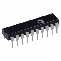
AD7112CN Analog Devices Inc, AD7112CN Datasheet - Page 10

AD7112CN
Manufacturer Part Number
AD7112CN
Description
IC DAC DUAL LOGARITHMIC 20-DIP
Manufacturer
Analog Devices Inc
Series
LOGDAC®r
Datasheet
1.AD7112BN.pdf
(12 pages)
Specifications of AD7112CN
Rohs Status
RoHS non-compliant
Number Of Bits
17
Data Interface
Parallel
Number Of Converters
2
Voltage Supply Source
Single Supply
Power Dissipation (max)
10mW
Operating Temperature
-40°C ~ 85°C
Mounting Type
Through Hole
Package / Case
20-DIP (0.300", 7.62mm)
Settling Time
-
AD7112
MICROPROCESSOR INTERFACING
Figures 18 to 20 show interfaces between the AD7112 and
three popular 8-bit microprocessor systems, the MC68008,
8085A/8088 and the 8051. In the MC68008 and 8085/8088 in-
terfaces, the AD7112 is memory mapped with separate ad-
dresses for each DAC.
AD7112-8085A/8088 INTERFACE
Figure 18 shows a connection diagram for interfacing the
AD7112 to both the 8085A and the 8088 microprocessors. This
scheme is also suited to the Z80 microprocessor, but the Z80
address/data bus does not have to be demultiplexed. The
AD7112 is memory mapped with separate memory addresses
for DAC A and DAC B.
AD7112–68008 INTERFACE
Figure 19 shows a connection diagram for interfacing the
AD7112 to the 68008 microprocessor. The AD7112 is again
memory mapped with separate memory addresses for DAC A
and DAC B.
8085A / 8088
68008
Figure 18. AD7112–8085A/8088 Interface Circuit
A23 – A1
AD7 – AD0
D7 – D0
DTACK
A15 – A8
Figure 19. AD7112–68008 Interface Circuit
R /W
AS
DEN
** A = DECODED ADDRESS FOR AD7112 DAC A
ALE
*
WR
ANALOG CIRCUITRY HAS BEEN OMITTED FOR CLARITY.
A+1 = DECODED ADDRESS FOR AD7112 DAC B
** A = DECODED ADDRESS FOR AD7112 DAC A
*
ANALOG CIRCUITRY HAS BEEN OMITTED FOR CLARITY.
A+1 = DECODED ADDRESS FOR AD7112 DAC B
LATCH
8-BIT
ADDRESS
DECODE
DATA BUS
LOGIC
ADDRESS BUS
A+1**
ADDRESS BUS
DATA BUS
ADDRESS
DECODE
LOGIC
A+1**
A **
A **
CS
DB7 – DB0
DAC A / DAC B
WR
AD7112*
DAC A / DAC B
CS
WR
DB7 – DB0
AD7112*
–10–
AD7112–8051 INTERFACE
Figure 20 shows a connection diagram between the AD7112
and the 8051 microprocessor. The AD7112 is port mapped in
this interface. The loading structure is as follows: Data to be
loaded to the DAC is output to Port 1: P3.0, P3.1 and P3.2 are
bit addressable port lines and are used to control the DAC
select, CS and WR inputs. A sample routine for writing to DAC A
is shown below.
MOV A,DATA; Data to be written is loaded to the accumulator.
CLR 3.2;
CLR 3.0;
CLR 3.1;
MOV A,P1;
SET B 3.1;
SET B 3.0;
APPLICATIONS
Automatic Gain Control
In an automatic gain control system an input signal is attenuated
or amplified so that its average output level remains constant.
The AD7112 D/A converter is used here as a variable gain or at-
tenuation element that adjusts the output signal relative to the
input level.
A feedback loop consisting of a detector, comparator, and up/
down counter continuously adjusts the contents of the counter
and hence the gain or attenuation of the circuit so that the signal
level at the output remains constant and equal to the reference
input signal. The negative feedback action of the loop ensures
that the average output voltage of the automatic gain control
system remains constant. Figure 21 shows a block diagram of a
typical AGC control loop using 1/2 AD7112 as the gain/ attenu-
ation element.
Whenever the input signal is outside the dynamic range of the
programmable gain element in the AGC loop, there should be a
stable, well defined input output relationship.
Figure 20. AD7112–8051 Interface Circuit
* ANALOG CIRCUITRY OMITTED FOR CLARITY
8051
Select DAC A.
Bring CS low.
Bring WR low.
Write data to DAC.
Deactivate WR.
Deactivate CS
P1.0
P1.1
P1.2
P1.3
P1.4
P1.5
P3.0
P3.1
P3.2
P1.6
P1.7
WR
DAC A / DAC B
CS
DB0
DB1
DB2
DB3
DB4
DB5
DB6
DB7
AD7112*
REV. 0


