AD7112CN Analog Devices Inc, AD7112CN Datasheet - Page 3
AD7112CN
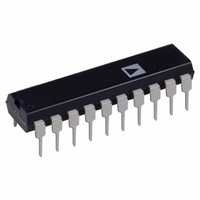
Manufacturer Part Number
AD7112CN
Description
IC DAC DUAL LOGARITHMIC 20-DIP
Manufacturer
Analog Devices Inc
Series
LOGDAC®r
Datasheet
1.AD7112BN.pdf
(12 pages)
Specifications of AD7112CN
Rohs Status
RoHS non-compliant
Number Of Bits
17
Data Interface
Parallel
Number Of Converters
2
Voltage Supply Source
Single Supply
Power Dissipation (max)
10mW
Operating Temperature
-40°C ~ 85°C
Mounting Type
Through Hole
Package / Case
20-DIP (0.300", 7.62mm)
Settling Time
-


REV. 0
TIMING SPECIFICATIONS
Parameter
CS to WR Setup Time
CS to WR Hold Time
DAC Select to WR Setup Time
DAC Select to WR Hold Time
Data Valid to WR Setup Time
Data Valid to WR Hold Time
WR Pulse Width
NOTES
1
Specifications subject to change without notice.
AC PERFORMANCE CHARACTERISTICS
Parameter
DC Supply Rejection
Digital-to-Analog Glitch Impulse
Output Capacitance, C
AC Feedthrough
Channel-to-Channel Isolation
Digital Feedthrough
Output Noise Voltage Density
Total Harmonic Distortion
NOTES
1
Specifications subject to change without notice.
Timing specifications guaranteed by design not production tested. All input signals are specified with tr = tf = 5 ns (10% to 90% of 5 V) and timed from a voltage
Guaranteed by design, not production tested.
level of 1.6 V.
V
V
V
V
(30 Hz to 50 kHz)
IN
IN
IN
IN
A to OUT A
B to OUT B
A to OUT B
B to OUT A
OUT A
Gain/ V
, C
OUT B
DD
1
t
t
t
t
t
t
t
(V
CS
CH
AS
AH
DS
DH
WR
T
+25 C
0.001
10
50
–94
–94
–87
–87
1
15
–91
DD
A
= +5 V
=
T
0
0
4
0
55
10
53
T
–40 C to
+85 C
0.005
10
50
–90
–90
–87
–87
1
15
–91
A
A
5%; 0UT A = OUT B = AGND = DGND = O V; V
= +25 C
=
1
(V
V
IN
DD
B = 10 V. Output amplifier AD712 except where noted.)
= +5 V
Units
dB/% max
nV s typ
pF max
dB max
dB max
dB typ
dB typ
nV s typ
nV/ Hz typ
dB typ
–3–
T
0
0
4
0
55
10
53
A
= –40 C to +85 C
5%; 0UT A = OUT B = AGND = DGND = 0 V; V
Conditions/Comments
Measured with AD843 as output amplifier for input
code transition 10000000 to 00000000.
V
Registers loaded with all 1s.
V
V
V
V
Measured with input code transitions of all 0s to all 1s.
Measured between R
R
V
Registers loaded with all 0s.
IN
IN
IN
IN
IN
IN
FB
V
DD
A, V
A = 6 V rms at 10 kHz sine wave,
B = 0 V. DAC Registers loaded with all 0s.
B = 6 V rms at 10 kHz sine wave,
A = 0 V. DAC Registers loaded with all 0s.
A = V
B and OUT B.
=
IN
IN
B = 6 V rms at 1 kHz. DAC
5%. Input Code = 00000000
B = 6 V rms at 1 kHz. DAC
IN
Units
ns min
ns min
ns min
ns min
ns min
ns min
ns min
A = V
FB
IN
B = 10 V)
A and OUT A or between
Conditions/Comments
See Figure 3.
IN
AD7112
A =
Related parts for AD7112CN
Image
Part Number
Description
Manufacturer
Datasheet
Request
R

Part Number:
Description:
±1.7g Dual-Axis IMEMS Accelerometer Evaluation Board
Manufacturer:
Analog Devices Inc
Datasheet:

Part Number:
Description:
Inertial Sensor Evaluation System
Manufacturer:
Analog Devices Inc
Datasheet:
Part Number:
Description:
Manufacturer:
Analog Devices Inc
Datasheet:
Part Number:
Description:
Manufacturer:
Analog Devices Inc
Datasheet:
Part Number:
Description:
Manufacturer:
Analog Devices Inc
Datasheet:
Part Number:
Description:
Manufacturer:
Analog Devices Inc
Datasheet:
Part Number:
Description:
Manufacturer:
Analog Devices Inc
Datasheet:
Part Number:
Description:
Manufacturer:
Analog Devices Inc
Datasheet:
Part Number:
Description:
Manufacturer:
Analog Devices Inc
Datasheet:
Part Number:
Description:
Manufacturer:
Analog Devices Inc
Datasheet:
Part Number:
Description:
Manufacturer:
Analog Devices Inc
Datasheet:
Part Number:
Description:
Manufacturer:
Analog Devices Inc
Datasheet:
Part Number:
Description:
Manufacturer:
Analog Devices Inc
Datasheet: