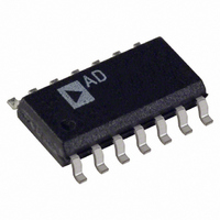
AD8303AR-REEL Analog Devices Inc, AD8303AR-REEL Datasheet - Page 12

AD8303AR-REEL
Manufacturer Part Number
AD8303AR-REEL
Description
IC DAC 12-BIT SERIAL 14-SOIC T/R
Manufacturer
Analog Devices Inc
Datasheet
1.AD8303AR.pdf
(16 pages)
Specifications of AD8303AR-REEL
Rohs Status
RoHS non-compliant
Settling Time
14µs
Number Of Bits
12
Data Interface
Serial, SPI™
Number Of Converters
2
Voltage Supply Source
Single Supply
Power Dissipation (max)
9.6mW
Operating Temperature
-40°C ~ 85°C
Mounting Type
Surface Mount
Package / Case
14-SOIC (3.9mm Width), 14-SOL
AD8303
BIPOLAR OUTPUT OPERATION
Although the AD8303 has been designed for single-supply
operation, the output can also be configured for bipolar
operation. A typical circuit is shown in Figure 31. This circuit
uses the AD8303’s internal voltage reference to generate a
bipolar offset. Since V
application, one half of an OP293 dual op amp is used as a
buffer. The other op amp then amplifies the DAC output
voltage to produce a bipolar output swing. The output voltage is
coded in offset binary and is given by:
where 0.5 mV represents the pretrimmed value for one LSB of
the AD8303, Digital Code is the digital code sent to the DAC,
and 1.0 V is the AD8303 reference voltage.
For a 2.048 V full scale using the circuit values shown, the
transfer function becomes:
Note that the full-scale span has increased from 2.048 V to
4.096 V ( 2.048 V). Therefore, although each AD8303 LSB
represents 0.5 mV, each output LSB of the bipolar circuit has
been scaled to 1 mV. The code table for this circuit is shown in
Table IV.
Hexadecimal Number Decimal Number
in DAC Register
FFF
801
800
7FF
000
As with the false-ground generator circuit, resistor matching is
V O
10
11
12
7
6
5
8
9
SDI
CLK
CS
LDA
LDB
RS
MSB
SHDN
AGND DGND
0.5 mV
1
AD8303
13
V
+3V
DD
Figure 31. Bipolar Output Operation
4
V
V
OUTA
V
OUTB
V O
REF
Digital Code
Table IV. Bipolar Code Table
3
14
2
1 mV
REF
OP293
1/2
10k
in DAC Register
4095
2049
2048
2047
0
R3
19.08k
must source current in this
Digital Code – 2.048 V
10k
R4
R1
R3 R4
OPTIONAL
FULL-SCALE
TRIM
R4
20.48k
R2
–3V
+3V
OP293
ZERO TRIM
OPTIONAL
1/2
1
Analog Output
Voltage (V)
2.047
0.001
0
–0.001
–2.048
R2
R1
– 1.0 V
V
OUT
= 2.048V
R2
R1
–12–
important to maintain accuracy. Resistor pairs R1-R2 and
R3-R4 should be selected to match within 0.01%. In addition,
these resistors must be of the same type (preferably metal film)
to insure temperature coefficient matching. Mismatching
between R1 and R2 causes offset and gain errors while an R3 to
R4 mismatch yields gain errors.
GENERATING A NEGATIVE SUPPLY VOLTAGE
Some applications may require a bipolar output configuration,
as shown in Figure 31, but only have a single power supply rail
available. This is very common in data acquisition systems using
microprocessor-based systems. In these systems, +12 V, +15 V,
and/or +5 V only are available. Single supply rails are, of course,
common in battery-powered systems. Shown in Figure 32 is a
method of generating a negative supply using a single IC and
two capacitors. The ADM8660 employs a charge pump
technique to invert supply voltages as low as 1.5 V. A shutdown
feature on the ADM8660 complements the shutdown of the
AD8303. Note, however, that the ADM8660 requires about
500 s to turn on after exiting the shutdown state.
MICROCOMPUTER INTERFACES
The AD8303 serial data input provides an easy interface to a
variety of single-chip microcomputers ( Cs). Many Cs have a
built-in serial data capability which can be used for communi-
cating with the DAC. In cases where no serial port is provided,
or it is being used for some other purpose (such as an RS-232
communications interface), the AD8303 can easily be addressed
in software.
Twelve data bits are required to load a value into the AD8303.
If more than 12 bits are transmitted before the Chip Select
input goes high, the extra (i.e., the most significant) bits are
ignored. This feature is valuable because most Cs only transmit
data in 8-bit increments. Thus, the C sends 16 bits to the DAC
instead of 12 bits. The AD8303 will only respond to the last 12
bits clocked into the SDI input, however, so the serial data
interface is not affected.
Figure 32. Generating a Negative Supply Voltage
10µF
SHDN FROM AD8303
2
4
CAP+
CAP–
6
LV
ADM8660
+3V
1
FC
V+
SHUTDOWN
74HC04
8
1/6
GND
3
OSC
5
7
10µF
–3V
REV. 0


