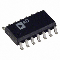
AD8303AR-REEL Analog Devices Inc, AD8303AR-REEL Datasheet - Page 13

AD8303AR-REEL
Manufacturer Part Number
AD8303AR-REEL
Description
IC DAC 12-BIT SERIAL 14-SOIC T/R
Manufacturer
Analog Devices Inc
Datasheet
1.AD8303AR.pdf
(16 pages)
Specifications of AD8303AR-REEL
Rohs Status
RoHS non-compliant
Settling Time
14µs
Number Of Bits
12
Data Interface
Serial, SPI™
Number Of Converters
2
Voltage Supply Source
Single Supply
Power Dissipation (max)
9.6mW
Operating Temperature
-40°C ~ 85°C
Mounting Type
Surface Mount
Package / Case
14-SOIC (3.9mm Width), 14-SOL
REV. 0
AD8303-MC68HC11 INTERFACE
The circuit illustrated in Figure 33 shows a serial interface
between the AD8303 and the MC68HC11 8-bit micro-
processor. The MOSI output drives the AD8303’s serial data
input, SDI, while SCK drives the clock (CLK). The DAC’s CS,
LDA, LDB, MSB and RS inputs are driven by lines PD5 and
PC0–PC3, respectively.
To load data into the AD8303, the 68HC11’s CPOL and
CPHA bits are set high. This action configures the C to
transfer data on the rising edge of the serial clock. After CS is
set low, two bytes of data are sent to the AD8303 using the
format shown in Figure 28. Then LDA or LDB are strobed low,
transferring the serial-input register contents to the appropriate
DAC. The RS and MSB inputs allow the DAC to be reset to
either zero volts or half scale at any time.
AN 8051 C INTERFACE
A typical interface between the AD8303 and an 8051 C is
shown in Figure 34. This interface also uses the C’s internal
serial port. The serial port is programmed for Mode 0
operation, which functions as a simple 8-bit shift register. The
8051’s Port 3.0 pin functions as the serial data output, while
Port 3.1 serves as the serial clock. The LDA and LDB pins are
controlled by the 8051’s Port 1.0 and Port 1.1 lines, respectively.
Figure 33. AD8303-MC68HC11 Serial Interface
Figure 34. AD8303-80CL51 Serial Interface
NOTE: ADDITIONAL PINS OMITTED FOR CLARITY
80CL51
NOTE: ADDITIONAL PINS OMITTED FOR CLARITY
MC68HC11
(P3.0) RxD
(P3.1) TxD
(PD3) MOSI
(PD4) SCK
(PD5) SS
V
P1.0
P1.1
DD
PC0
PC1
PC2
PC3
10k
1µF
10
7
6
8
RS CS
SDI
CLK
LDA
LDB
+
9
SDI
CLK
CS
LDA
LDB
MSB
RS
5
MSB
AD8303
AD8303
11
SHDN
12
V
DD
–13–
The 8051’s serial data transmission is straightforward. When
data is written to the serial buffer register (SBUF, at Special
Function Register location 99H), the data is automatically
converted to serial format and clocked out via Port 3.0 and Port
3.1 After 8 bits have been transmitted, the Transmit Interrupt
flag (SCON.1) is set and the next 8 bits can be transmitted.
The circuit of Figure 34 demonstrates “hardwiring” many of the
AD8303 features which may not have to be changed within a
given design. For example, the reset feature is controlled by a
resistor and capacitor. This produces a power-on reset pulse
without requiring a C I/O pin. The MSB pin can be hardwired
to V
scale is required. If the AD8303 is the only device on the serial
interface, CS can also be tied to ground. Finally, SHDN can be
tied to V
Software for the interface of Figure 34 is shown in Figure 35.
This routine sends the 12-bit value placed in registers
DAC_VAL0 and DAC_VAL1 to the DAC addressed by the two
LSBs of DAC_ADDR.
The subroutine begins by setting appropriate bits in the Serial
Control register to configure the serial port for Mode 0
operation. The MSBs of the DAC value are obtained from
memory location DAC_VAL1, adjusted to compensate for the
8051’s serial data format, and moved to the serial buffer
register. At this point, serial data transmission begins
automatically. When all 8 bits have been sent, the Transmit
Interrupt bit is set, and the subroutine then proceeds to send the
LSBs of the DAC value, stored at location DAC_VAL0. Next
the LDA and LDB bits from DAC_ADDR are logically ANDed
with Port1. This action sets the appropriate AD8303 DAC
select input low and transfers the DAC value from the serial-
input register to the DAC register, causing the DAC output
voltage to change. Finally the LDA and LDB inputs are driven
high to await the next DAC update.
The 8051 sends data out of its shift register LSB first, while the
AD8303 requires data MSB first. The subroutine therefore
includes a BYTESWAP subroutine to reformat the data. This
routine transfers the MSB-first byte at location SHIFTREG to
an LSB-first byte at location SENDBYTE. The routine rotates
the MSB of the first byte into the carry with a Rotate Left Carry
instruction, then rotates the carry into the MSB of the second
byte with a Rotate Right Carry instruction. After 8 loops,
SENDBYTE contains the data in the proper format. The
BYTESWAP routine in Listing C is convenient because the
DAC data can be calculated in normal LSB form.
DD
or ground, depending on whether a reset to 0 V or half
DD
if the shutdown feature will not be used.
AD8303


