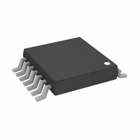
AD8303JRU Analog Devices Inc, AD8303JRU Datasheet - Page 2

AD8303JRU
Manufacturer Part Number
AD8303JRU
Description
IC DAC 12-BIT SERIAL 14-SOIC
Manufacturer
Analog Devices Inc
Datasheet
1.AD8303AR.pdf
(16 pages)
Specifications of AD8303JRU
Rohs Status
RoHS non-compliant
Settling Time
14µs
Number Of Bits
12
Data Interface
Serial, SPI™
Number Of Converters
2
Voltage Supply Source
Single Supply
Power Dissipation (max)
9.6mW
Operating Temperature
-40°C ~ 85°C
Mounting Type
Surface Mount
Package / Case
14-TSSOP
+3 V OPERATION
Parameter
STATIC PERFORMANCE
ANALOG OUTPUTS
REFERENCE OUTPUT
LOGIC INPUTS
INTERFACE TIMING SPECIFICATIONS
AC CHARACTERISTICS
SUPPLY CHARACTERISTICS
NOTES
1
2
3
4
5
6
7
Specifications subject to change without notice.
AD8303–SPECIFICATIONS
Typical readings represent the average value of room temperature operation.
1 LSB = 0.5 mV for 0 V to +2.0475 V output range. The first two codes (000
Includes internal voltage reference error.
These parameters are guaranteed by design and not subject to production testing.
All input control signals are specified with t
The settling time specification does not apply for negative going transitions within the last 6 LSBs of ground.
See Figure 6 for a plot of incremental supply current consumption as a function of the digital input voltage levels.
Resolution
Relative Accuracy
Differential Nonlinearity
Differential Nonlinearity
Zero-Scale Error
Full-Scale Voltage
Full-Scale Tempco
Output Current
Output Resistance to GND
Capacitive Load
Output Voltage
Logic Input Low Voltage
Logic Input High Voltage
Input Leakage Current
Input Capacitance
Clock Width High
Clock Width Low
Load Pulse Width
Data Setup
Data Hold
Reset Pulse Width
Load Setup
Load Hold
Select
Deselect
Output Slew Rate
Power Supply Sensitivity
Voltage Output Settling Time
Voltage Output Settling Time
Shutdown Recovery Time
DAC Glitch
Digital Feedthrough
Power Supply Range
Shutdown Current
Supply Current
Power Dissipation
2
7
4
2
3
4
3, 4
2
2
4
(@ V
6
6
DD
= +2.7 V to +3.6 V, –40 C
R
= t
F
= 2 ns (10% to 90% of +3 V) and timed from a voltage level of 1.6 V.
4, 5
Symbol
N
INL
DNL
DNL
V
V
TCV
I
R
C
V
V
V
I
C
t
t
t
t
t
t
t
t
t
t
t
t
t
SR
Q
Q
V
I
I
P
PSS
OUT
IL
CH
CL
LDW
DS
DH
RS
LD1
LD2
CSS
CSH
S
S
DSR
DD_SD
DD
DISS
ZSE
FS
OUT
IL
IH
DD RANGE
L
REF
IL
FS
Monotonic, T
Monotonic
Data = 000
Condition
Data = 000
Data = FFF
Data = 800
Data = 000
No Oscillation
Load > 1 M
To 0.1% of Full Scale
To 1 LSB of Final Value
To 0.1% of Full Scale
DNL < 1 LSB
SHDN = 0, No Load, V
V
V
V
DD
DD
DD
= 3 V, V
= 3 V, V
T
H
A
= 5%
, 001
–2–
+85 C, unless otherwise noted)
H
H
H
H
H
) are excluded from the linearity error measurement.
H
, V
IL
IL
2
to FFFH to 000
A
3
= 0 V, No Load
= 0 V, No Load
= +25 C
OUT
< 3 mV
IL
= 0 V, T
H
A
= +25 C
Min Typ
12
–2
–3/4
–1
2.039 2.0475 2.056 Volts
2.1
40
40
40
15
15
40
15
40
40
40
2.7
1.25
16
30
500
1
4
14
10
2.0
15
15
0.02
2
6
0.001 0.004 %/%
1/2
1/4
1/2
1
Max Units
+2
+3/4
+1
+4.5
0.6
10
10
5.5
1
3.2
9.6
3
Bits
LSB
LSB
LSB
mV
ppm/ C
mA
pF
V
V
V
pF
ns
ns
ns
ns
ns
ns
ns
ns
ns
ns
V/ s
nV/s
V
nV/s
mA
mW
REV. 0
A
s
s
s
A


