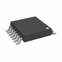
AD8303JRU Analog Devices Inc, AD8303JRU Datasheet - Page 5

AD8303JRU
Manufacturer Part Number
AD8303JRU
Description
IC DAC 12-BIT SERIAL 14-SOIC
Manufacturer
Analog Devices Inc
Datasheet
1.AD8303AR.pdf
(16 pages)
Specifications of AD8303JRU
Rohs Status
RoHS non-compliant
Settling Time
14µs
Number Of Bits
12
Data Interface
Serial, SPI™
Number Of Converters
2
Voltage Supply Source
Single Supply
Power Dissipation (max)
9.6mW
Operating Temperature
-40°C ~ 85°C
Mounting Type
Surface Mount
Package / Case
14-TSSOP
REV. 0
CS
H
L
L
L
H
H
X
X
X
X
X
NOTES
1
2
Pin No.
1
2
3
4
5
6
7
8
9
10
11
12
13
14
Do not clock in serial data while LDA or LDB is LOW.
+
+ positive logic transition; – negative logic transition; X Don’t Care.
CLK RS
X
L
H
L
X
X
X
X
X
X
X
+
Name
AGND
V
V
DGND
CS
CLK
SDI
LDA
RS
LDB
MSB
SHDN
V
V
H
H
H
H
H
H
H
L
L
X
OUTA
REF
DD
OUTB
+
+
MSB SHDN LDA/B Serial Shift Register Function
X
X
X
X
X
X
X
H
H
L
X
X
Function
Analog Ground.
DAC voltage output, 2.0475 V full scale with 0.5 mV per bit. An internal temperature stabilized reference
maintains a fixed full-scale voltage independent of time, temperature and power supply variations.
Reference Voltage Output Terminal. Very high output resistance must be buffered if used as a virtual
ground.
Digital Ground
Chip Select, Active Low Input. Disables shift register loading when high. Does not effect LDA or LDB
operation.
Clock Input, positive edge clocks data into shift register.
Serial Data Input, input data loads directly into the shift register.
Load DAC register strobes, active low. Transfers shift register data to DAC A register. Asynchronous active
low input. See Control Logic Truth Table for operation.
Resets DAC register to zero condition or half-scale depending on MSB pin. Asynchronous active low input.
Load DAC register strobes, active low. Transfers shift register data to DAC B register. Asynchronous active
low input. See Control Logic Truth Table for operation.
Digital Input: Logic High presets DAC registers to half-scale 800
is strobed; Logic Low clears all DAC registers to zero (000
Active low shutdown control input. Does not affect register contents as long as power is present on V
Positive power supply input. Specified range of operation +2.7 V to +5.5 V
DAC voltage output, 2.0475 V full scale with 0.5 mV per bit. An internal temperature stabilized reference
maintains a fixed full-scale voltage independent of time, temperature and power supply variations.
H
H
H
H
H
H
H
H
H
H
H
L
H
H
H
H
H
L
X
H
X
H
X
–
No Effect
No Effect
No Effect
Shift-Register-Data Advanced One Bit Latched
No Effect
No Effect
No Effect
No Effect
No Effect
No Effect
No Effect
No Effect
Table I. Control-Logic Truth Table
PIN CONFIGURATION
V
AGND
DGND
PIN DESCRIPTIONS
OUTA
V
14-Lead SOIC (R-14)
CLK
14-Pin P-DIP (N-14)
REF
SDI
CS
1
2
3
4
5
6
7
(Not to Scale)
AD8303
TOP VIEW
–5–
14
13
12
10
11
9
8
V
V
SHDN
MSB
LDB
RS
LDA
OUTB
DD
H
) when the RS pin is strobed.
DAC Register Function
Latched
Latched
Latched
Latched
Updated with Current Shift Register Contents
Transparent
Loaded with 800
Latched with 800
Loaded with All Zeros
Latched All Zeros
No Effect
H
(sets MSB bit to one) when the RS pin
H
H
AD8303
DD
.


