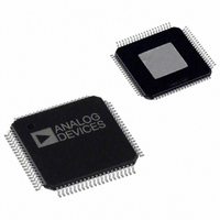
AD9786BSVRL Analog Devices Inc, AD9786BSVRL Datasheet - Page 10

AD9786BSVRL
Manufacturer Part Number
AD9786BSVRL
Description
IC DAC 16BIT INTERPOL/SP 80TQFP
Manufacturer
Analog Devices Inc
Series
TxDAC+®r
Datasheet
1.AD9786BSVZRL.pdf
(56 pages)
Specifications of AD9786BSVRL
Number Of Bits
16
Data Interface
Parallel
Number Of Converters
1
Voltage Supply Source
Single Supply
Power Dissipation (max)
1.25W
Operating Temperature
-40°C ~ 85°C
Mounting Type
Surface Mount
Package / Case
80-TQFP Exposed Pad, 80-eTQFP, 80-HTQFP, 80-VQFP
For Use With
AD9786-EB - BOARD EVALUATION FOR AD9786
Lead Free Status / RoHS Status
Contains lead / RoHS non-compliant
Settling Time
-
AD9786
ANALOG
Table 7. Analog Pin Function Descriptions
Pin No.
59
60
70, 71
61
62, 79
63, 78
64, 77
65, 76
66, 75
67, 74
68, 73
69, 72
80
DATA
Table 8. Data Pin Function Descriptions
Pin No.
10 to 15, 18 to
24, 27 to 29
32
33
34, 37 to 43,
46 to 51
30
9, 17, 26,
36, 44, 52
8, 16, 25,
35, 45, 53
P1B15 to P1B0
IQSEL/P2B15
ONEPORTCLOCK/P2B14
P2B13 to P2B0
DRVDD
DVDD
DGND
Mnemonic
Mnemonic
REFIO
FSADJ
IOUTB, IOUTA
DNC
ADVDD
ADGND
ACVDD
ACGND
AVDD2
AGND2
AVDD1
AGND1
DNC
Direction
I
I
I/O
I
Direction
A
A
A
Description
Input Data Port 1.
ONEPORT
0x02[6]
0
1
ONEPORT
0x02[6]
0
1
1
1
1
ONEPORT
0x02[6]
0
1
Input Data Port 2, Bit 13 to Bit 0.
Digital Output Pin Supply, 3.3 V.
Digital Domain, 2.5 V.
Digital Domain, 0 V.
Rev. B | Page 10 of 56
Description
Reference.
Full-Scale Adjust.
Differential DAC Output Currents.
Do Not Connect.
Analog Domain Digital Content 2.5 V.
Analog Domain Digital Content 0 V.
Analog Domain Clock Content 2.5 V.
Analog Domain Clock Content 0 V.
Analog Domain Clock Switching 3.3 V.
Analog Domain Switching 0 V.
Analog Domain Quiet 3.3 V.
Analog Domain Quiet 0 V.
Do Not Connect.
Mode
Latched data routed for I channel processing.
Latched data demultiplexed by IQSEL and routed for
interleaved I/Q processing.
IQPOL
0x02[1]
X
0
0
1
1
Latched data routed for Q channel Bit 14 processing.
Pin configured for output of clock at twice the channel
data route.
IQSEL/
P2B15
X
0
1
0
1
Mode (IQPOL = 0)
Latched data routed to Q channel Bit 15
(MSB) processing.
Latched data on Data Port 1 routed to Q
channel processing.
Latched data on Data Port 1 routed to I
channel processing.
Latched data on Data Port 1 routed to I
channel processing.
Latched data on Data Port 1 routed to Q
channel processing.


