EPM570T100C4N Altera, EPM570T100C4N Datasheet - Page 55
EPM570T100C4N
Manufacturer Part Number
EPM570T100C4N
Description
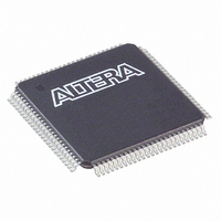
IC MAX II CPLD 570 LE 100-TQFP
Manufacturer
Altera
Series
MAX® IIr
Specifications of EPM570T100C4N
Programmable Type
In System Programmable
Delay Time Tpd(1) Max
5.4ns
Voltage Supply - Internal
2.5V, 3.3V
Number Of Logic Elements/blocks
570
Number Of Macrocells
440
Number Of I /o
76
Operating Temperature
0°C ~ 85°C
Mounting Type
Surface Mount
Package / Case
100-TQFP, 100-VQFP
Voltage
2.5V, 3.3V
Memory Type
FLASH
Number Of Logic Elements/cells
570
No. Of I/o's
76
Propagation Delay
7ns
Global Clock Setup Time
1.5ns
Frequency
247.5MHz
Supply Voltage Range
2.375V To 2.625V, 3V To 3.6V
Operating Temperature Range
0°C To +85°C
Rohs Compliant
Yes
No. Of Macrocells
440
Lead Free Status / RoHS Status
Lead free / RoHS Compliant
Features
-
Other names
544-1316
EPM570T100C4N
EPM570T100C4N
Available stocks
Company
Part Number
Manufacturer
Quantity
Price
Company:

Part Number:
EPM570T100C4N
Manufacturer:
ALTERA
Quantity:
1 143


Chapter 4: Hot Socketing and Power-On Reset in MAX II Devices
Power-On Reset Circuitry
Figure 4–4. ESD Protection During Negative Voltage Zap
Power-On Reset Circuitry
© October 2008 Altera Corporation
When the I/O pin receives a negative ESD zap at the pin that is less than –0.7 V (0.7 V
is the voltage drop across a diode), the intrinsic
P-Substrate/N+ drain diode is forward biased. Therefore, the discharge ESD current
path is from GND to the I/O pin, as shown in
MAX II devices have POR circuits to monitor V
power-up. The POR circuit monitors these voltages, triggering download from the
non-volatile configuration flash memory (CFM) block to the SRAM logic, maintaining
tri-state of the I/O pins (with weak pull-up resistors enabled) before and during this
process. When the MAX II device enters user mode, the POR circuit releases the I/O
pins to user functionality. The POR circuit of the MAX II (except MAX IIZ) device
continues to monitor the V
POR circuit of the MAX IIZ device does not monitor the V
device enters into user mode. More details are provided in the following sub-sections.
I/O
GND
Source
Drain
Drain
Source
CCINT
PMOS
NMOS
voltage level to detect a brown-out condition. The
Gate
Gate
P-Substrate
Figure
CCINT
N+
N+
and V
D
S
4–4.
GND
I/O
G
CCIO
CCINT
voltage levels during
voltage level after the
MAX II Device Handbook
4–5
Related parts for EPM570T100C4N
Image
Part Number
Description
Manufacturer
Datasheet
Request
R

Part Number:
Description:
CYCLONE II STARTER KIT EP2C20N
Manufacturer:
Altera
Datasheet:


Part Number:
Description:
CPLD, EP610 Family, ECMOS Process, 300 Gates, 16 Macro Cells, 16 Reg., 16 User I/Os, 5V Supply, 35 Speed Grade, 24DIP
Manufacturer:
Altera Corporation
Datasheet:
Part Number:
Description:
CPLD, EP610 Family, ECMOS Process, 300 Gates, 16 Macro Cells, 16 Reg., 16 User I/Os, 5V Supply, 15 Speed Grade, 24DIP
Manufacturer:
Altera Corporation
Datasheet:
Part Number:
Description:
Manufacturer:
Altera Corporation
Datasheet:
Part Number:
Description:
CPLD, EP610 Family, ECMOS Process, 300 Gates, 16 Macro Cells, 16 Reg., 16 User I/Os, 5V Supply, 30 Speed Grade, 24DIP
Manufacturer:
Altera Corporation
Datasheet:
Part Number:
Description:
High-performance, low-power erasable programmable logic devices with 8 macrocells, 10ns
Manufacturer:
Altera Corporation
Datasheet:
Part Number:
Description:
High-performance, low-power erasable programmable logic devices with 8 macrocells, 7ns
Manufacturer:
Altera Corporation
Datasheet:
Part Number:
Description:
Classic EPLD
Manufacturer:
Altera Corporation
Datasheet:
Part Number:
Description:
High-performance, low-power erasable programmable logic devices with 8 macrocells, 10ns
Manufacturer:
Altera Corporation
Datasheet:
Part Number:
Description:
Manufacturer:
Altera Corporation
Datasheet:
Part Number:
Description:
Manufacturer:
Altera Corporation
Datasheet:
Part Number:
Description:
Manufacturer:
Altera Corporation
Datasheet:
Part Number:
Description:
CPLD, EP610 Family, ECMOS Process, 300 Gates, 16 Macro Cells, 16 Reg., 16 User I/Os, 5V Supply, 25 Speed Grade, 24DIP
Manufacturer:
Altera Corporation
Datasheet: