EPM570F100C4N Altera, EPM570F100C4N Datasheet - Page 31
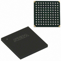
EPM570F100C4N
Manufacturer Part Number
EPM570F100C4N
Description
IC MAX II CPLD 570 LE 100-FBGA
Manufacturer
Altera
Series
MAX® IIr
Specifications of EPM570F100C4N
Programmable Type
In System Programmable
Delay Time Tpd(1) Max
5.4ns
Voltage Supply - Internal
2.5V, 3.3V
Number Of Logic Elements/blocks
570
Number Of Macrocells
440
Number Of I /o
76
Operating Temperature
0°C ~ 85°C
Mounting Type
Surface Mount
Package / Case
100-FBGA
Voltage
2.5V, 3.3V
Memory Type
FLASH
Number Of Logic Elements/cells
570
Family Name
MAX II
# Macrocells
440
Frequency (max)
2.3148GHz
Propagation Delay Time
7ns
Number Of Logic Blocks/elements
57
# I/os (max)
76
Operating Supply Voltage (typ)
2.5/3.3V
In System Programmable
Yes
Operating Supply Voltage (min)
2.375V
Operating Supply Voltage (max)
3.6V
Operating Temp Range
0C to 85C
Operating Temperature Classification
Commercial
Mounting
Surface Mount
Pin Count
100
Package Type
FBGA
No. Of I/o's
76
Propagation Delay
7ns
Global Clock Setup Time
1.5ns
Frequency
247.5MHz
Supply Voltage Range
2.375V To 2.625V, 3V To 3.6V
Operating Temperature Range
0°C To +85°C
Rohs Compliant
Yes
Lead Free Status / RoHS Status
Lead free / RoHS Compliant
Features
-
Lead Free Status / Rohs Status
Compliant
Other names
544-1716
Available stocks
Company
Part Number
Manufacturer
Quantity
Price
Company:

Part Number:
EPM570F100C4N
Manufacturer:
ALTERA
Quantity:
12 388
Company:
Part Number:
EPM570F100C4N
Manufacturer:
ALTERA
Quantity:
325
Part Number:
EPM570F100C4N
Manufacturer:
ALTERA/阿尔特拉
Quantity:
20 000


Chapter 2: MAX II Architecture
I/O Structure
I/O Structure
Fast I/O Connection
© October 2008 Altera Corporation
IOEs support many features, including:
■
■
■
■
■
■
■
■
■
■
■
■
■
■
MAX II device IOEs contain a bidirectional I/O buffer.
IOE structure. Registers from adjacent LABs can drive to or be driven from the IOE’s
bidirectional I/O buffers. The Quartus II software automatically attempts to place
registers in the adjacent LAB with fast I/O connection to achieve the fastest possible
clock-to-output and registered output enable timing. For input registers, the
Quartus II software automatically routes the register to guarantee zero hold time.
You can set timing assignments in the Quartus II software to achieve desired I/O
timing.
A dedicated fast I/O connection from the adjacent LAB to the IOEs within an I/O
block provides faster output delays for clock-to-output and t
This connection exists for data output signals, not output enable signals or input
signals.
LVTTL and LVCMOS I/O standards
3.3-V, 32-bit, 66-MHz PCI compliance
Joint Test Action Group (JTAG) boundary-scan test (BST) support
Programmable drive strength control
Weak pull-up resistors during power-up and in system programming
Slew-rate control
Tri-state buffers with individual output enable control
Bus-hold circuitry
Programmable pull-up resistors in user mode
Unique output enable per pin
Open-drain outputs
Schmitt trigger inputs
Fast I/O connection
Programmable input delay
Figure
2–20,
Figure
2–21, and
Figure 2–22
illustrate the fast I/O connection.
Figure 2–19
PD
propagation delays.
shows the MAX II
MAX II Device Handbook
2–23
Related parts for EPM570F100C4N
Image
Part Number
Description
Manufacturer
Datasheet
Request
R

Part Number:
Description:
CYCLONE II STARTER KIT EP2C20N
Manufacturer:
Altera
Datasheet:


Part Number:
Description:
CPLD, EP610 Family, ECMOS Process, 300 Gates, 16 Macro Cells, 16 Reg., 16 User I/Os, 5V Supply, 35 Speed Grade, 24DIP
Manufacturer:
Altera Corporation
Datasheet:
Part Number:
Description:
CPLD, EP610 Family, ECMOS Process, 300 Gates, 16 Macro Cells, 16 Reg., 16 User I/Os, 5V Supply, 15 Speed Grade, 24DIP
Manufacturer:
Altera Corporation
Datasheet:
Part Number:
Description:
Manufacturer:
Altera Corporation
Datasheet:
Part Number:
Description:
CPLD, EP610 Family, ECMOS Process, 300 Gates, 16 Macro Cells, 16 Reg., 16 User I/Os, 5V Supply, 30 Speed Grade, 24DIP
Manufacturer:
Altera Corporation
Datasheet:
Part Number:
Description:
High-performance, low-power erasable programmable logic devices with 8 macrocells, 10ns
Manufacturer:
Altera Corporation
Datasheet:
Part Number:
Description:
High-performance, low-power erasable programmable logic devices with 8 macrocells, 7ns
Manufacturer:
Altera Corporation
Datasheet:
Part Number:
Description:
Classic EPLD
Manufacturer:
Altera Corporation
Datasheet:
Part Number:
Description:
High-performance, low-power erasable programmable logic devices with 8 macrocells, 10ns
Manufacturer:
Altera Corporation
Datasheet:
Part Number:
Description:
Manufacturer:
Altera Corporation
Datasheet:
Part Number:
Description:
Manufacturer:
Altera Corporation
Datasheet:
Part Number:
Description:
Manufacturer:
Altera Corporation
Datasheet:
Part Number:
Description:
CPLD, EP610 Family, ECMOS Process, 300 Gates, 16 Macro Cells, 16 Reg., 16 User I/Os, 5V Supply, 25 Speed Grade, 24DIP
Manufacturer:
Altera Corporation
Datasheet: