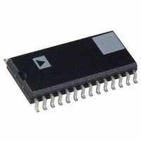
ADMCF326BR Analog Devices Inc, ADMCF326BR Datasheet - Page 16

ADMCF326BR
Manufacturer Part Number
ADMCF326BR
Description
IC DSP FLASH MOTOR CTRLR 28SOIC
Manufacturer
Analog Devices Inc
Series
Motor Controlr
Type
Fixed Pointr
Datasheet
1.ADMCF326BN.pdf
(36 pages)
Specifications of ADMCF326BR
Rohs Status
RoHS non-compliant
Interface
Synchronous Serial Port (SSP)
Clock Rate
20MHz
Non-volatile Memory
FLASH (12 kB), ROM (12kB)
On-chip Ram
2.5kB
Voltage - I/o
5.00V
Voltage - Core
5.00V
Operating Temperature
-40°C ~ 85°C
Mounting Type
Surface Mount
Package / Case
28-SOIC (7.5mm Width)
Available stocks
Company
Part Number
Manufacturer
Quantity
Price
Part Number:
ADMCF326BR
Manufacturer:
ADI/亚德诺
Quantity:
20 000
Company:
Part Number:
ADMCF326BRZ
Manufacturer:
SHARP
Quantity:
1 000
Part Number:
ADMCF326BRZ
Manufacturer:
ADI/亚德诺
Quantity:
20 000
ADMCF326
same time. In the control of an ECM, one inverter leg (Phase C
in this example) is disabled for a number of PWM cycles. This
disable may be implemented by disabling both the CH and CL
PWM outputs by setting Bits 0 and 1 of the PWMSEG Register.
This is illustrated in Figure 9, where it can be seen that both
the AH and BL signals are identical, because PWMCHA =
PWMCHB, and the crossover bit for Phase B is set. In addition,
the other four signals (AL, BH, CH, and CL) have been disabled
by setting the appropriate enable/disable bits of the PWMSEG
Register. For the situation illustrated in Figure 9, the appropri-
ate value for the PWMSEG Register is 0x00A7. In ECM operation,
because each inverter leg is disabled for certain periods of time,
the PWMSEG Register is changed based upon the position of
the rotor shaft (motor commutation).
Figure 9. An example of PWM signals suitable for ECM
control. PWMCHA = PWMCHB, BH/BL are a crossover pair.
AL, BH, CH, and CL outputs are disabled. Operation is in
Single Update Mode.
Gate Drive Unit: PWMGATE Register
The gate drive unit of the PWM controller adds features that
simplify the design of isolated gate drive circuits for PWM
inverters. If a transformer-coupled power device gate drive ampli-
fier is used, the active PWM signal must be chopped at a high
frequency. The PWMGATE Register allows the programming
of this high frequency chopping mode. The chopped active
PWM signals may be required for the high side drivers only,
for the low side drivers only, or for both the high side and
low side switches. Therefore, independent control of this mode
for both high and low side switches is included with two separate
control bits in the PWMGATE Register.
Typical PWM output signals with high frequency chopping
enabled on both high side and low side signals are shown in
Figure 10. Chopping of the high side PWM outputs (AH, BH,
and CH) is enabled by setting Bit 8 of the PWMGATE Register.
Chopping of the low side PWM outputs (AL, BL, and CL) is
AH
BH
CH
AL
BL
CL
2
PWMDT
PWMTM
= PWMCHB
PWMCHA
= PWMCHB
PWMCHA
PWMTM
2
PWMDT
–16–
enabled by setting Bit 9 of the PWMGATE Register. The high
chopping frequency is controlled by the 8-bit word (GDCLK)
written to Bits 0 to 7 of the PWMGATE Register. The period
and the frequency of this high frequency carrier are:
The GDCLK value may range from 0 to 255, corresponding
to a programmable chopping frequency rate from 19.5 kHz to
5 MHz for a 20 MHz CLKOUT rate. The gate drive features
must be programmed before operation of the PWM controller
and typically are not changed during normal operation of the
PWM controller. Following a reset, by default, all bits of the
PWMGATE Register are cleared so that high frequency chopping
is disabled.
Figure 10. Typical PWM signals with high frequency gate
chopping enabled on both high side and low side switches
(GDCLK is the integer equivalent of the value in Bits 0 to 7
of the PWMGATE Register.)
PWM Shutdown
In the event of external fault conditions, it is essential that the
PWM system be instantaneously shut down. Two methods of
sensing a fault condition are provided by the ADMCF326. For
the first method, a low level on the PWMTRIP pin initiates
an instantaneous, asynchronous (independent of DSP clock)
shutdown of the PWM controller. This places all six PWM
outputs in the OFF state, disables the PWMSYNC pulse and
associated interrupt signal, and generates a PWMTRIP interrupt
signal. The PWMTRIP pin has an internal pull-down resistor so
that even if the pin becomes disconnected, the PWM outputs will
be disabled. The state of the PWMTRIP pin can be read from
Bit 0 of the SYSSTAT Register.
It is possible through software to initiate a PWM shutdown by
writing to the 1-bit read/write PWMSWT Register (0x2061).
Writing to this bit generates a PWM shutdown in a manner
identical to the PWMTRIP pin. Following a PWM shutdown,
it is possible to determine if the shutdown was generated from
hardware or software by reading the same PWMSWT Register.
Reading this register also clears it.
2
PWMDT
[4
T
PWMTM
CHOP
(GDCLK+1)
f
CHOP
=
PWMCHA
[
4
=
×
[
4
t
CK
(
GDCLK
×
]
(
GDCLK
f
CLKOUT
PWMCHA
+
1
)
+
PWMTM
]
1
×
)
]
t
CK
2
PWMDT
REV. B


