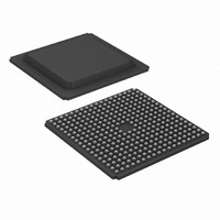
XC3S500E-4FGG320C Xilinx Inc, XC3S500E-4FGG320C Datasheet - Page 88

XC3S500E-4FGG320C
Manufacturer Part Number
XC3S500E-4FGG320C
Description
IC SPARTAN-3E FPGA 500K 320FBGA
Manufacturer
Xilinx Inc
Series
Spartan™-3Er
Datasheet
1.XC3S100E-4VQG100C.pdf
(233 pages)
Specifications of XC3S500E-4FGG320C
Total Ram Bits
368640
Number Of Logic Elements/cells
10476
Number Of Labs/clbs
1164
Number Of I /o
232
Number Of Gates
500000
Voltage - Supply
1.14 V ~ 1.26 V
Mounting Type
Surface Mount
Operating Temperature
0°C ~ 85°C
Package / Case
320-BGA
No. Of Logic Blocks
10476
No. Of Gates
500000
No. Of Macrocells
10476
No. Of Speed Grades
4
No. Of I/o's
250
Clock Management
DLL
Package
320FBGA
Family Name
Spartan®-3E
Device Logic Cells
10476
Device Logic Units
1164
Device System Gates
500000
Number Of Registers
9312
Maximum Internal Frequency
572 MHz
Typical Operating Supply Voltage
1.2 V
Maximum Number Of User I/os
232
Ram Bits
368640
Lead Free Status / RoHS Status
Lead free / RoHS Compliant
For Use With
122-1536 - KIT STARTER SPARTAN-3E
Lead Free Status / RoHS Status
Lead free / RoHS Compliant, Lead free / RoHS Compliant
Other names
122-1526
Available stocks
Company
Part Number
Manufacturer
Quantity
Price
Company:
Part Number:
XC3S500E-4FGG320C
Manufacturer:
XILINX
Quantity:
913
Company:
Part Number:
XC3S500E-4FGG320C
Manufacturer:
XILINX
Quantity:
745
Company:
Part Number:
XC3S500E-4FGG320C
Manufacturer:
Xilinx Inc
Quantity:
10 000
Company:
Part Number:
XC3S500E-4FGG320C
Manufacturer:
XILINX
Quantity:
2 000
Part Number:
XC3S500E-4FGG320C
Manufacturer:
XILINX/赛灵思
Quantity:
20 000
Functional Description
Table 59: Byte-Wide Peripheral Interface (BPI) Connections (Continued)
88
LDC1
HDC
LDC2
A[23:0]
D[7:0]
CSO_B
BUSY
D
Pin Name
FPGA Direction
Output
Output
Output
Output
Output
Output
Input
PROM Output Enable
PROM Write Enable
PROM Byte Mode
Address
Data Input
Chip Select Output. Active Low.
Busy Indicator. Typically only
used after configuration, if
bitstream option Persist=Yes.
Description
www.xilinx.com
Connect to the PROM
output-enable input (OE#). The
FPGA drives this signal Low
throughout configuration.
Connect to PROM write-enable
input (WE#). FPGA drives this
signal High throughout
configuration.
This signal is not used for x8
PROMs. For PROMs with a x8/x16
data width control, connect to
PROM byte-mode input (BYTE#).
See
Flash
signal Low throughout
configuration.
Connect to PROM address inputs.
High-order address lines may not
be available in all packages and
not all may be required. Number of
address lines required depends
on the size of the attached Flash
PROM. FPGA address generation
controlled by M0 mode pin.
Addresses presented on falling
CCLK edge.
Only 20 address lines are
available in TQ144 package.
FPGA receives byte-wide data on
these pins in response the
address presented on A[23:0].
Data captured by FPGA on rising
edge of CCLK.
Not used in single FPGA
applications. In a daisy-chain
configuration, this pin connects to
the CSI_B pin of the next FPGA in
the chain. If HSWAP = 1 in a
multi-FPGA daisy-chain
application, connect this signal to
a 4.7 kΩ pull-up resistor to
VCCO_2. Actively drives Low
when selecting a downstream
device in the chain.
Not used during configuration but
actively drives.
Precautions Using x8/x16
During Configuration
PROMs. FPGA drives this
DS312-2 (v3.8) August 26, 2009
User I/O
User I/O
User I/O. Drive this pin
High after configuration to
use a x8/x16 PROM in x16
mode.
User I/O
User I/O. If bitstream
option Persist=Yes,
becomes part of
SelectMap parallel
peripheral interface.
User I/O
User I/O. If bitstream
option Persist=Yes,
becomes part of
SelectMap parallel
peripheral interface.
After Configuration
Product Specification
R


