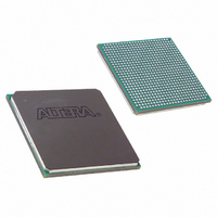
EP2S15F672C5 Altera, EP2S15F672C5 Datasheet - Page 216

EP2S15F672C5
Manufacturer Part Number
EP2S15F672C5
Description
IC STRATIX II FPGA 15K 672-FBGA
Manufacturer
Altera
Series
Stratix® IIr
Datasheet
1.EP2S15F484I4N.pdf
(238 pages)
Specifications of EP2S15F672C5
Number Of Logic Elements/cells
15600
Number Of Labs/clbs
780
Total Ram Bits
419328
Number Of I /o
366
Voltage - Supply
1.15 V ~ 1.25 V
Mounting Type
Surface Mount
Operating Temperature
0°C ~ 85°C
Package / Case
672-FBGA
Family Name
Stratix II
Number Of Logic Blocks/elements
15600
# I/os (max)
366
Frequency (max)
609.76MHz
Process Technology
90nm (CMOS)
Operating Supply Voltage (typ)
1.2V
Logic Cells
15600
Ram Bits
419328
Operating Supply Voltage (min)
1.15V
Operating Supply Voltage (max)
1.25V
Operating Temp Range
0C to 85C
Operating Temperature Classification
Commercial
Mounting
Surface Mount
Pin Count
672
Package Type
FC-FBGA
Lead Free Status / RoHS Status
Contains lead / RoHS non-compliant
Number Of Gates
-
Lead Free Status / Rohs Status
Not Compliant
Other names
544-1124
Available stocks
Company
Part Number
Manufacturer
Quantity
Price
Company:
Part Number:
EP2S15F672C5
Manufacturer:
ALTERA
Quantity:
1 238
Part Number:
EP2S15F672C5
Manufacturer:
ALTERA/阿尔特拉
Quantity:
20 000
Company:
Part Number:
EP2S15F672C5N
Manufacturer:
EXAR
Quantity:
56
Company:
Part Number:
EP2S15F672C5N
Manufacturer:
ALTERA
Quantity:
390
Duty Cycle Distortion
5–80
Stratix II Device Handbook, Volume 1
Here is an example for calculating the DCD as a percentage for a
non-DDIO output on a row I/O on a -3 device:
If the non-DDIO output I/O standard is SSTL-2 Class II, the maximum
DCD is 95 ps (see
period T is:
To calculate the DCD as a percentage:
Note to
(1)
1.8 V
1.5-V LVCMOS
SSTL-2 Class I
SSTL-2 Class II
SSTL-18 Class I
1.8-V HSTL Class I
1.5-V HSTL Class I
LVDS/
HyperTransport
technology
Table 5–80. Maximum DCD for Non-DDIO Output on Row I/O Pins (Part 2
of 2)
Row I/O Output
T = 1/ f = 1 / 267 MHz = 3.745 ns = 3745 ps
boundary)
boundary)
The DCD specification is based on a no logic array noise condition.
(T/2 – DCD) / T = (3745ps/2 – 95ps) / 3745ps = 47.5% (for low
(T/2 + DCD) / T = (3745ps/2 + 95ps) / 3745ps = 52.5% (for high
Standard
Table
Note (1)
5–80:
Table
5–80). If the clock frequency is 267 MHz, the clock
-3 Devices
180
165
115
95
55
80
85
55
Maximum DCD for Non-DDIO Output
-4 & -5 Devices
180
195
145
125
100
115
85
80
Altera Corporation
Unit
April 2011
ps
ps
ps
ps
ps
ps
ps
ps


