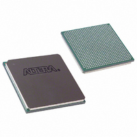
EP1S40F780C7 Altera, EP1S40F780C7 Datasheet - Page 143

EP1S40F780C7
Manufacturer Part Number
EP1S40F780C7
Description
IC STRATIX FPGA 40K LE 780-FBGA
Manufacturer
Altera
Series
Stratix®r
Datasheet
1.EP1S10F780C7.pdf
(276 pages)
Specifications of EP1S40F780C7
Number Of Logic Elements/cells
41250
Number Of Labs/clbs
4125
Total Ram Bits
3423744
Number Of I /o
615
Voltage - Supply
1.425 V ~ 1.575 V
Mounting Type
Surface Mount
Operating Temperature
0°C ~ 85°C
Package / Case
780-FBGA
Lead Free Status / RoHS Status
Contains lead / RoHS non-compliant
Number Of Gates
-
Other names
544-1429
EP1S40SF780C7
EP1S40SF780C7
Available stocks
Company
Part Number
Manufacturer
Quantity
Price
Company:
Part Number:
EP1S40F780C7
Manufacturer:
ALTERA
Quantity:
355
Company:
Part Number:
EP1S40F780C7
Manufacturer:
ALTERA
Quantity:
648
Part Number:
EP1S40F780C7
Manufacturer:
ALTERA/阿尔特拉
Quantity:
20 000
Altera Corporation
July 2005
Notes to
(1)
(2)
(3)
R
Table 2–35. Differential On-Chip Termination
Symbol
D
(2)
Data measured over minimum conditions (T
V
Data measured over minimum conditions (T
V
LVDS data rate is supported for 840 Mbps using internal differential termination.
C C I O
CCIO
Table
= –5%).
= –5%).
Internal differential termination for LVDS
2–35:
Description
However, there is additional resistance present between the device ball
and the input of the receiver buffer, as shown in
resistance is because of package trace resistance (which can be calculated
as the resistance from the package ball to the pad) and the parasitic layout
metal routing resistance (which is shown between the pad and the
intersection of the on-chip termination and input buffer).
Figure 2–72. Differential Resistance of LVDS Differential Pin Pair (R
Table 2–35
commercial devices.
MultiVolt I/O Interface
The Stratix architecture supports the MultiVolt I/O interface feature,
which allows Stratix devices in all packages to interface with systems of
different supply voltages.
The Stratix VCCINT pins must always be connected to a 1.5-V power
supply. With a 1.5-V V
3.3-V tolerant. The VCCIO pins can be connected to either a 1.5-V, 1.8-V,
2.5-V, or 3.3-V power supply, depending on the output requirements.
defines the specification for internal termination resistance for
Package Ball
R
D
j
j
= –40 C, V
= 0 C, V
0.3 Ω
0.3 Ω
CCINT
C C I O
CCIO
Pad
Commercial (1),
Industrial (2),
+5%) and maximum conditions (T
+5%) and maximum conditions (T
level, input pins are 1.5-V, 1.8-V, 2.5-V, and
9.3 Ω
9.3 Ω
Conditions
(3)
Stratix Device Handbook, Volume 1
(3)
Input Buffer
LVDS
Differential On-Chip
Termination Resistor
Figure
Min
110
100
Resistance
Stratix Architecture
2–72. This
j
135
135
Typ
= 85 C,
j
= 100 C,
Max
165
170
D
)
2–129
Unit
W
W


