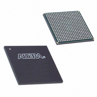
EP1C4F400C7 Altera, EP1C4F400C7 Datasheet - Page 87

EP1C4F400C7
Manufacturer Part Number
EP1C4F400C7
Description
IC CYCLONE FPGA 4K LE 400-FBGA
Manufacturer
Altera
Series
Cyclone®r
Datasheet
1.EP1C3T144C8.pdf
(106 pages)
Specifications of EP1C4F400C7
Number Of Logic Elements/cells
4000
Number Of Labs/clbs
400
Total Ram Bits
78336
Number Of I /o
301
Voltage - Supply
1.425 V ~ 1.575 V
Mounting Type
Surface Mount
Operating Temperature
0°C ~ 85°C
Package / Case
400-FBGA
Family Name
Cyclone®
Number Of Logic Blocks/elements
4000
# I/os (max)
301
Frequency (max)
320.1MHz
Process Technology
0.13um (CMOS)
Operating Supply Voltage (typ)
1.5V
Logic Cells
4000
Ram Bits
78336
Operating Supply Voltage (min)
1.425V
Operating Supply Voltage (max)
1.575V
Operating Temp Range
0C to 85C
Operating Temperature Classification
Commercial
Mounting
Surface Mount
Pin Count
400
Package Type
FBGA
Lead Free Status / RoHS Status
Contains lead / RoHS non-compliant
Number Of Gates
-
Lead Free Status / Rohs Status
Not Compliant
Other names
544-2079
Available stocks
Company
Part Number
Manufacturer
Quantity
Price
Company:
Part Number:
EP1C4F400C7
Manufacturer:
TI
Quantity:
150
Company:
Part Number:
EP1C4F400C7
Manufacturer:
ALTERA
Quantity:
3 000
Company:
Part Number:
EP1C4F400C7N
Manufacturer:
ALTERA
Quantity:
784
Part Number:
EP1C4F400C7N
Manufacturer:
ALTERA
Quantity:
20 000
Altera Corporation
May 2008
Notes to
(1)
(2)
t
O U T C O P L L
Table 4–29. Cyclone Global Clock External I/O Timing Parameters
Symbol
These timing parameters are sample-tested only.
These timing parameters are for IOE pins using a 3.3-V LVTTL, 24-mA setting. Designers should use the Quartus II
software to verify the external timing for any pin.
Table
4–29:
Clock-to-output delay output or bidirectional pin using IOE
output register with global clock enhanced PLL with default
phase setting
Tables 4–30
and row pins for EP1C3 devices.
t
t
t
t
t
t
t
t
t
t
t
t
I N S U
I N H
O U T C O
I N S U P L L
I N H P L L
O U T C O P L L
I N S U
I N H
O U T C O
I N S U P L L
I N H P L L
O U T C O P L L
Table 4–30. EP1C3 Column Pin Global Clock External I/O Timing
Parameters
Table 4–31. EP1C3 Row Pin Global Clock External I/O Timing Parameters
Symbol
Symbol
Parameter
through
-6 Speed Grade
-6 Speed Grade
3.085
0.000
2.000
1.795
0.000
0.500
3.157
0.000
2.000
1.867
0.000
0.500
Min
Min
4–31
4.073
2.306
3.984
2.217
Max
Max
—
—
—
—
—
—
—
—
show the external timing parameters on column
-7 Speed Grade
-7 Speed Grade
3.547
0.000
2.000
2.063
0.000
0.500
3.630
0.000
2.000
2.146
0.000
0.500
Min
Min
Notes
4.682
2.651
4.580
2.549
Max
Max
—
—
—
—
—
—
—
—
C
LOAD
(1),
(2)
= 10 pF
-8 Speed Grade
-8 Speed Grade
4.009
0.000
2.000
2.332
0.000
0.500
4.103
0.000
2.000
2.426
0.000
0.500
Min
Min
(Part 2 of 2)
Conditions
5.295
2.998
5.180
2.883
Max
Max
Timing Model
—
—
—
—
—
—
—
—
Preliminary
Unit
Unit
ns
ns
ns
ns
ns
ns
ns
ns
ns
ns
ns
ns
4–17


