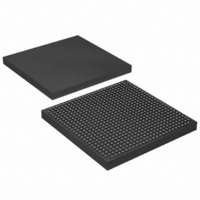
EP1S10F672C7 Altera, EP1S10F672C7 Datasheet - Page 78

EP1S10F672C7
Manufacturer Part Number
EP1S10F672C7
Description
IC STRATIX FPGA 10K LE 672-FBGA
Manufacturer
Altera
Series
Stratix®r
Datasheet
1.EP1S10F780C7.pdf
(276 pages)
Specifications of EP1S10F672C7
Number Of Logic Elements/cells
10570
Number Of Labs/clbs
1057
Total Ram Bits
920448
Number Of I /o
345
Voltage - Supply
1.425 V ~ 1.575 V
Mounting Type
Surface Mount
Operating Temperature
0°C ~ 85°C
Package / Case
672-FBGA
Family Name
Stratix
Number Of Logic Blocks/elements
10570
# I/os (max)
345
Frequency (max)
420.17MHz
Process Technology
0.13um (CMOS)
Operating Supply Voltage (typ)
1.5V
Logic Cells
10570
Ram Bits
920448
Operating Supply Voltage (min)
1.425V
Operating Supply Voltage (max)
1.575V
Operating Temp Range
0C to 85C
Operating Temperature Classification
Commercial
Mounting
Surface Mount
Pin Count
672
Package Type
FBGA
Lead Free Status / RoHS Status
Contains lead / RoHS non-compliant
Number Of Gates
-
Lead Free Status / Rohs Status
Not Compliant
Other names
544-1109
Available stocks
Company
Part Number
Manufacturer
Quantity
Price
Company:
Part Number:
EP1S10F672C7
Manufacturer:
ALTERA
Quantity:
3 000
Part Number:
EP1S10F672C7
Manufacturer:
XILINX/赛灵思
Quantity:
20 000
Company:
Part Number:
EP1S10F672C7AA
Manufacturer:
ALTERA
Quantity:
3 000
Company:
Part Number:
EP1S10F672C7ES
Manufacturer:
ALTERA
Quantity:
89
Company:
Part Number:
EP1S10F672C7N
Manufacturer:
ALTERA
Quantity:
3 000
Part Number:
EP1S10F672C7N
Manufacturer:
ALTERA/阿尔特拉
Quantity:
20 000
Digital Signal Processing Block
2–64
Stratix Device Handbook, Volume 1
Output Selection Multiplexer
The outputs from the various elements of the adder/output block are
routed through an output selection multiplexer. Based on the DSP block
operational mode and user settings, the multiplexer selects whether the
output from the multiplier, the adder/subtractor/accumulator, or
summation block feeds to the output.
Output Registers
Optional output registers for the DSP block outputs are controlled by four
sets of control signals: clock[3..0], aclr[3..0], and ena[3..0].
Output registers can be used in any mode.
Modes of Operation
The adder, subtractor, and accumulate functions of a DSP block have four
modes of operation:
■
■
■
■
1
Simple Multiplier Mode
In simple multiplier mode, the DSP block drives the multiplier sub-block
result directly to the output with or without an output register. Up to four
18 × 18-bit multipliers or eight 9 × 9-bit multipliers can drive their results
directly out of one DSP block. See
Simple multiplier
Multiply-accumulator
Two-multipliers adder
Four-multipliers adder
Each DSP block can only support one mode. Mixed modes in the
same DSP block is not supported.
Figure
2–35.
Altera Corporation
July 2005


