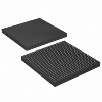
EP1S20F672I7N Altera, EP1S20F672I7N Datasheet - Page 269

EP1S20F672I7N
Manufacturer Part Number
EP1S20F672I7N
Description
IC STRATIX FPGA 20K LE 672-FBGA
Manufacturer
Altera
Series
Stratix®r
Datasheet
1.EP1S10F780C7.pdf
(276 pages)
Specifications of EP1S20F672I7N
Number Of Logic Elements/cells
18460
Number Of Labs/clbs
1846
Total Ram Bits
1669248
Number Of I /o
426
Voltage - Supply
1.425 V ~ 1.575 V
Mounting Type
Surface Mount
Operating Temperature
-40°C ~ 100°C
Package / Case
672-FBGA
Lead Free Status / RoHS Status
Lead free / RoHS Compliant
Number Of Gates
-
Available stocks
Company
Part Number
Manufacturer
Quantity
Price
Company:
Part Number:
EP1S20F672I7N
Manufacturer:
ALTERA20
Quantity:
212
- Current page: 269 of 276
- Download datasheet (4Mb)
Altera Corporation
January 2006
Notes to
(1)
(2)
(3)
(4)
(5)
(6)
(7)
(8)
(9)
(10) Exact, user-controllable value depends on the PLL settings.
(11) The LOCK circuit on Stratix PLLs does not work for industrial devices below -20C unless the PFD frequency > 200
t
t
f
% spread
t
LSKEW
SKEW
SS
ARESET
Table 4–130. Enhanced PLL Specifications for -8 Speed Grade (Part 3 of 3)
Symbol
The minimum input clock frequency to the PFD (f
Use this equation (f
to determine the allowed PLL settings.
See
t
This parameter is timing analyzed by the Quartus II software because the scanclk and scandata ports can be
driven by the logic array.
Actual jitter performance may vary based on the system configuration.
Total required time to reconfigure and lock is equal to t
changed, then t
When using the spread-spectrum feature, the minimum VCO frequency is 500 MHz. The maximum VCO
frequency is determined by the speed grade selected.
Lock time is a function of PLL configuration and may be significantly faster depending on bandwidth settings or
feedback counter change increment.
MHz. See the Stratix FPGA Errata Sheet for more information on the PLL.
FCOMP
“Maximum Input & Output Clock Rates” on page
Tables 4–127
can also equal 50% of the input clock period multiplied by the pre-scale divider n (whichever is less).
Clock skew between two external
clock outputs driven by the same
counter
Clock skew between two external
clock outputs driven by the different
counters with the same settings
Spread spectrum modulation
frequency
Percentage spread for spread
spectrum frequency
Minimum pulse width on
signal
DLOCK
through 4–130:
OUT
is equal to 0.
= f
Parameter
I N
* ml(n × post-scale counter)) in conjunction with the specified f
(10)
areset
IN
/N) must be at least 3 MHz for Stratix device enhanced PLLs.
Min
0.5
30
10
4–76.
DLOCK
±50
±75
Typ
+ t
CONFIG
. If only post-scale counters and delays are
Stratix Device Handbook, Volume 1
DC & Switching Characteristics
Max
150
0.6
I N P F D
and f
V C O
ranges
Unit
kHz
ps
ps
ns
%
4–99
Related parts for EP1S20F672I7N
Image
Part Number
Description
Manufacturer
Datasheet
Request
R

Part Number:
Description:
CYCLONE II STARTER KIT EP2C20N
Manufacturer:
Altera
Datasheet:

Part Number:
Description:
CPLD, EP610 Family, ECMOS Process, 300 Gates, 16 Macro Cells, 16 Reg., 16 User I/Os, 5V Supply, 35 Speed Grade, 24DIP
Manufacturer:
Altera Corporation
Datasheet:

Part Number:
Description:
CPLD, EP610 Family, ECMOS Process, 300 Gates, 16 Macro Cells, 16 Reg., 16 User I/Os, 5V Supply, 15 Speed Grade, 24DIP
Manufacturer:
Altera Corporation
Datasheet:

Part Number:
Description:
Manufacturer:
Altera Corporation
Datasheet:

Part Number:
Description:
CPLD, EP610 Family, ECMOS Process, 300 Gates, 16 Macro Cells, 16 Reg., 16 User I/Os, 5V Supply, 30 Speed Grade, 24DIP
Manufacturer:
Altera Corporation
Datasheet:

Part Number:
Description:
High-performance, low-power erasable programmable logic devices with 8 macrocells, 10ns
Manufacturer:
Altera Corporation
Datasheet:

Part Number:
Description:
High-performance, low-power erasable programmable logic devices with 8 macrocells, 7ns
Manufacturer:
Altera Corporation
Datasheet:

Part Number:
Description:
Classic EPLD
Manufacturer:
Altera Corporation
Datasheet:

Part Number:
Description:
High-performance, low-power erasable programmable logic devices with 8 macrocells, 10ns
Manufacturer:
Altera Corporation
Datasheet:

Part Number:
Description:
Manufacturer:
Altera Corporation
Datasheet:

Part Number:
Description:
Manufacturer:
Altera Corporation
Datasheet:

Part Number:
Description:
Manufacturer:
Altera Corporation
Datasheet:

Part Number:
Description:
CPLD, EP610 Family, ECMOS Process, 300 Gates, 16 Macro Cells, 16 Reg., 16 User I/Os, 5V Supply, 25 Speed Grade, 24DIP
Manufacturer:
Altera Corporation
Datasheet:


