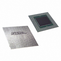
EP20K400EBC652-3N Altera, EP20K400EBC652-3N Datasheet - Page 32

EP20K400EBC652-3N
Manufacturer Part Number
EP20K400EBC652-3N
Description
IC APEX 20KE FPGA 400K 652-BGA
Manufacturer
Altera
Series
APEX-20K®r
Datasheet
1.EP20K30ETC144-3.pdf
(117 pages)
Specifications of EP20K400EBC652-3N
Number Of Logic Elements/cells
16640
Number Of Labs/clbs
1664
Total Ram Bits
212992
Number Of I /o
488
Number Of Gates
1052000
Voltage - Supply
1.71 V ~ 1.89 V
Mounting Type
Surface Mount
Operating Temperature
0°C ~ 85°C
Package / Case
652-BGA
Family Name
APEX 20K
Number Of Usable Gates
400000
Number Of Logic Blocks/elements
16640
# I/os (max)
488
Frequency (max)
213MHz
Process Technology
SRAM
Operating Supply Voltage (typ)
1.8V
Logic Cells
16640
Ram Bits
212992
Device System Gates
1052000
Operating Supply Voltage (min)
1.71V
Operating Supply Voltage (max)
1.89V
Operating Temp Range
0C to 85C
Operating Temperature Classification
Commercial
Mounting
Surface Mount
Pin Count
652
Package Type
BGA
Lead Free Status / RoHS Status
Lead free / RoHS Compliant
Available stocks
Company
Part Number
Manufacturer
Quantity
Price
APEX 20K Programmable Logic Device Family Data Sheet
Figure 20. ESB in Read/Write Clock Mode
Notes to
(1)
(2)
32
wraddress[ ]
rdaddress[ ]
outclocken
inclocken
outclock
Dedicated Clocks
inclock
All registers can be cleared asynchronously by ESB local interconnect signals, global signals, or the chip-wide reset.
APEX 20KE devices have four dedicated clocks.
data[ ]
wren
rden
Figure
(2)
2 or 4
Dedicated Inputs &
Global Signals
20:
4
Read/Write Clock Mode
The read/write clock mode contains two clocks. One clock controls all
registers associated with writing: data input, WE, and write address. The
other clock controls all registers associated with reading: read enable
(RE), read address, and data output. The ESB also supports clock enable
and asynchronous clear signals; these signals also control the read and
write registers independently. Read/write clock mode is commonly used
for applications where reads and writes occur at different system
frequencies.
D
ENA
D
ENA
D
ENA
Figure 20
Q
Q
Q
Note (1)
D
ENA
D
ENA
Generator
shows the ESB in read/write clock mode.
Pulse
Write
Q
Q
Data In
Read Address
Write Address
Read Enable
Write Enable
RAM/ROM
1,024 × 2
2,048 × 1
Data Out
128 × 16
256 × 8
512 × 4
D
ENA
Q
Altera Corporation
To MegaLAB,
FastTrack &
Local
Interconnect


