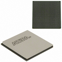
EP2SGX90EF1152C3ES Altera, EP2SGX90EF1152C3ES Datasheet - Page 182

EP2SGX90EF1152C3ES
Manufacturer Part Number
EP2SGX90EF1152C3ES
Description
IC STRATIX II GX 90K 1152-FBGA
Manufacturer
Altera
Series
Stratix® II GXr
Datasheet
1.EP2SGX30DF780C5.pdf
(316 pages)
Specifications of EP2SGX90EF1152C3ES
Number Of Logic Elements/cells
90960
Number Of Labs/clbs
4548
Total Ram Bits
4520448
Number Of I /o
558
Voltage - Supply
1.15 V ~ 1.25 V
Mounting Type
Surface Mount
Operating Temperature
0°C ~ 70°C
Package / Case
1152-FBGA
For Use With
544-1725 - PCIE KIT W/S II GX EP2SGX90N544-1724 - SI KIT W/SII GX EP2SGX90N544-1702 - VIDEO KIT W/SII GX EP2SGX90N
Lead Free Status / RoHS Status
Contains lead / RoHS non-compliant
Number Of Gates
-
Other names
544-1763
Available stocks
Company
Part Number
Manufacturer
Quantity
Price
- Current page: 182 of 316
- Download datasheet (2Mb)
Operating Conditions
Figure 4–4. Transmitter Output Waveform
Figure 4–5. Maximum Receiver Input Pin Voltage
Note to
(1)
4–12
Stratix II GX Device Handbook, Volume 1
Note to
(1)
V
Table 4–7. Typical V
V
OD
C C H
The absolute V
Typical (mV)
Applicable to data rates from 600 Mbps to 6.375 Gbps. Specification is for measurement at the package ball.
TX = 1.5 V
Figure
Table
Single-Ended Waveform
Differential Waveform
Single-Ended Waveform
4–7:
4–5:
MAX
V MAX = V CM + V
OD
that the receiver input pins can tolerate is 2 V.
200
220
Setting, TX Term = 100 Ω
V
Tables 4–7
600 Mbps to 6.375 Gbps. The specification is for measurement at the
package ball.
CM
V
CM = 0.85 V
V
V
(single-ended p-p)max
(single-ended p-p)max
OD
400
430
2
through
V
OD
= 3.3 V/2
= 0.85 + 0.825 = 1.675 V (1)
600
625
Note (1)
4–12
V OD (diff peak-peak) = 2 x V OD (single-ended)
V
show the typical V
OD
Setting (mV)
800
830
V
OD
1000
1020
p − n = 0 V
Positive Channel (p)
Negative Channel (n)
Ground
Positive Channel (p)
Negative Channel (n)
Ground
OD
for data rates from
1200
1200
Altera Corporation
June 2009
1400
1350
Related parts for EP2SGX90EF1152C3ES
Image
Part Number
Description
Manufacturer
Datasheet
Request
R

Part Number:
Description:
CYCLONE II STARTER KIT EP2C20N
Manufacturer:
Altera
Datasheet:

Part Number:
Description:
CPLD, EP610 Family, ECMOS Process, 300 Gates, 16 Macro Cells, 16 Reg., 16 User I/Os, 5V Supply, 35 Speed Grade, 24DIP
Manufacturer:
Altera Corporation
Datasheet:

Part Number:
Description:
CPLD, EP610 Family, ECMOS Process, 300 Gates, 16 Macro Cells, 16 Reg., 16 User I/Os, 5V Supply, 15 Speed Grade, 24DIP
Manufacturer:
Altera Corporation
Datasheet:

Part Number:
Description:
Manufacturer:
Altera Corporation
Datasheet:

Part Number:
Description:
CPLD, EP610 Family, ECMOS Process, 300 Gates, 16 Macro Cells, 16 Reg., 16 User I/Os, 5V Supply, 30 Speed Grade, 24DIP
Manufacturer:
Altera Corporation
Datasheet:

Part Number:
Description:
High-performance, low-power erasable programmable logic devices with 8 macrocells, 10ns
Manufacturer:
Altera Corporation
Datasheet:

Part Number:
Description:
High-performance, low-power erasable programmable logic devices with 8 macrocells, 7ns
Manufacturer:
Altera Corporation
Datasheet:

Part Number:
Description:
Classic EPLD
Manufacturer:
Altera Corporation
Datasheet:

Part Number:
Description:
High-performance, low-power erasable programmable logic devices with 8 macrocells, 10ns
Manufacturer:
Altera Corporation
Datasheet:

Part Number:
Description:
Manufacturer:
Altera Corporation
Datasheet:

Part Number:
Description:
Manufacturer:
Altera Corporation
Datasheet:

Part Number:
Description:
Manufacturer:
Altera Corporation
Datasheet:

Part Number:
Description:
CPLD, EP610 Family, ECMOS Process, 300 Gates, 16 Macro Cells, 16 Reg., 16 User I/Os, 5V Supply, 25 Speed Grade, 24DIP
Manufacturer:
Altera Corporation
Datasheet:


