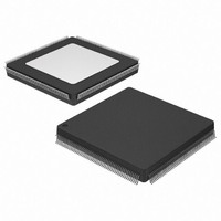
XC3S400-4PQG208I Xilinx Inc, XC3S400-4PQG208I Datasheet - Page 72

XC3S400-4PQG208I
Manufacturer Part Number
XC3S400-4PQG208I
Description
SPARTAN-3A FPGA 400K STD 208PQFP
Manufacturer
Xilinx Inc
Series
Spartan™-3r
Datasheet
1.XC3S50-4VQG100C.pdf
(217 pages)
Specifications of XC3S400-4PQG208I
Number Of Logic Elements/cells
8064
Number Of Labs/clbs
896
Total Ram Bits
294912
Number Of I /o
141
Number Of Gates
400000
Voltage - Supply
1.14 V ~ 1.26 V
Mounting Type
Surface Mount
Operating Temperature
-40°C ~ 100°C
Package / Case
208-BFQFP
Package
208PQFP
Family Name
Spartan®-3
Device Logic Units
8064
Device System Gates
400000
Maximum Internal Frequency
630 MHz
Typical Operating Supply Voltage
1.2 V
Maximum Number Of User I/os
141
Ram Bits
294912
Lead Free Status / RoHS Status
Lead free / RoHS Compliant
Available stocks
Company
Part Number
Manufacturer
Quantity
Price
Company:
Part Number:
XC3S400-4PQG208I
Manufacturer:
ATMEL
Quantity:
1 000
Part Number:
XC3S400-4PQG208I
Manufacturer:
XILINX/赛灵思
Quantity:
20 000
Spartan-3 FPGA Family: DC and Switching Characteristics
Table 44: Timing for the IOB Output Path
72
Notes:
1.
2.
3.
Clock-to-Output Times
Propagation Times
Set/Reset Times
T
Symbol
The numbers in this table are tested using the methodology presented in
forth in
This time requires adjustment whenever a signal standard other than LVCMOS25 with 12 mA drive and Fast slew rate is assigned
to the data Output. When this is true, add the appropriate Output adjustment from
For minimums, use the values reported by the Xilinx timing analyzer.
T
T
T
T
IOGSRQ
IOCKP
IOOLP
IOSRP
IOOP
Table 31
When reading from the Output
Flip-Flop (OFF), the time from the
active transition at the OTCLK
input to data appearing at the
Output pin
The time it takes for data to travel
from the IOB’s O input to the
Output pin
The time it takes for data to travel
from the O input through the OFF
latch to the Output pin
Time from asserting the OFF’s SR
input to setting/resetting data at
the Output pin
Time from asserting the Global
Set Reset (GSR) net to
setting/resetting data at the
Output pin
and
Table
34.
Description
www.xilinx.com
LVCMOS25
output drive, Fast slew rate
LVCMOS25
output drive, Fast slew rate
LVCMOS25
output drive, Fast slew rate
Conditions
(2)
(2)
(2)
, 12mA
, 12mA
, 12mA
Table 47
Table
and are based on the operating conditions set
XC3S200
XC3S400
XC3S50
XC3S1000
XC3S1500
XC3S2000
XC3S4000
XC3S5000
XC3S200
XC3S400
XC3S50
XC3S1000
XC3S1500
XC3S2000
XC3S4000
XC3S5000
XC3S200
XC3S400
XC3S50
XC3S1000
XC3S1500
XC3S2000
XC3S4000
XC3S5000
XC3S200
XC3S400
XC3S50
XC3S1000
XC3S1500
XC3S2000
XC3S4000
XC3S5000
46.
Device
All
DS099-3 (v2.5) December 4, 2009
Speed Grade
Max
1.28
1.95
1.28
1.94
1.28
1.95
2.10
2.77
8.07
-5
Product Specification
Max
1.47
2.24
1.46
2.23
1.47
2.24
2.41
3.18
9.28
-4
Units
ns
ns
ns
ns
ns
ns
ns
ns
ns
R


