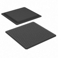
XC3SD1800A-4FGG676C Xilinx Inc, XC3SD1800A-4FGG676C Datasheet - Page 16

XC3SD1800A-4FGG676C
Manufacturer Part Number
XC3SD1800A-4FGG676C
Description
SPARTAN-3ADSP FPGA 1800K 676FBGA
Manufacturer
Xilinx Inc
Series
Spartan™-3A DSPr
Datasheets
1.XC3S50A-4VQG100C.pdf
(7 pages)
2.XC3SD3400A-4FGG676C.pdf
(4 pages)
3.XC3SD3400A-4FGG676C.pdf
(101 pages)
Specifications of XC3SD1800A-4FGG676C
Total Ram Bits
1548288
Number Of Logic Elements/cells
37440
Number Of Labs/clbs
4160
Number Of I /o
519
Number Of Gates
1800000
Voltage - Supply
1.14 V ~ 1.26 V
Mounting Type
Surface Mount
Operating Temperature
0°C ~ 85°C
Package / Case
676-BBGA
No. Of Logic Blocks
4224
No. Of Gates
1800000
No. Of Macrocells
37440
Family Type
Spartan-3A
No. Of Speed Grades
4
No. Of I/o's
519
Clock
RoHS Compliant
Lead Free Status / RoHS Status
Lead free / RoHS Compliant
For Use With
122-1574 - KIT DEVELOPMENT SPARTAN 3ADSP
Lead Free Status / RoHS Status
Lead free / RoHS Compliant
Other names
122-1538
Available stocks
Company
Part Number
Manufacturer
Quantity
Price
Company:
Part Number:
XC3SD1800A-4FGG676C
Manufacturer:
XILINX
Quantity:
853
Company:
Part Number:
XC3SD1800A-4FGG676C
Manufacturer:
Xilinx Inc
Quantity:
10 000
Company:
Part Number:
XC3SD1800A-4FGG676C
Manufacturer:
XILINX
Quantity:
160
Differential I/O Standards
Differential Input Pairs
X-Ref Target - Figure 3
Table 12: Recommended Operating Conditions for User I/Os Using Differential Signal Standards
DS610 (v3.0) October 4, 2010
Product Specification
Notes:
1.
2.
3.
4.
5.
6.
7.
8.
9.
LVDS_25
LVDS_33
BLVDS_25
MINI_LVDS_25
MINI_LVDS_33
LVPECL_25
LVPECL_33
RSDS_25
RSDS_33
TMDS_33
PPDS_25
PPDS_33
DIFF_HSTL_I_18
DIFF_HSTL_II_18
DIFF_HSTL_III_18
DIFF_HSTL_I
DIFF_HSTL_III
DIFF_SSTL18_I
DIFF_SSTL18_II
DIFF_SSTL2_I
DIFF_SSTL2_II
DIFF_SSTL3_I
DIFF_SSTL3_II
IOSTANDARD Attribute
The V
V
These true differential output standards are supported only on FPGA banks 0 and 2. Inputs are unrestricted. See the chapter "Using I/O Resources" in UG331.
See
LVPECL is supported on inputs only, not outputs. LVPECL_33 requires V
LVPECL_33 maximum V
Requires V
These higher-drive output standards are supported only on FPGA banks 1 and 3. Inputs are unrestricted. See the chapter "Using I/O Resources" in UG331.
All standards except for LVPECL and TMDS can have VCCAUX at either 2.5V or 3.3V. Define your VCCAUX level using the CONFIG VCCAUX constraint.
ICM
"External Termination Requirements for Differential I/O."
must be less than V
CCO
(3)
(3)
(3)
(3)
(3)
(3)
(
3
(4)
,
(5)
(5)
4
rails supply only differential output drivers, not input circuits.
,
CCAUX
7
)
(3)
(3)
(8)
(8)
(8)
= 3.3V ±10%. (V
ICM
CCAUX
= the lower of 2.8V or V
.
Min (V)
CCAUX
2.25
2.25
2.25
2.25
3.14
2.25
3.0
3.0
3.0
3.0
1.7
1.7
1.7
1.4
1.4
1.7
1.7
2.3
2.3
3.0
3.0
Internal
GND level
Logic
- 300 mV) ≤ V
V
CCO
V
V
Inputs Only
Inputs Only
INN
INP
Nom (V)
for Drivers
2.5
3.3
2.5
2.5
3.3
2.5
3.3
3.3
2.5
3.3
1.8
1.8
1.8
1.5
1.5
1.8
1.8
2.5
2.5
3.3
3.3
CCAUX
Figure 3: Differential Input Voltages
V
ICM
V
ICM
ID
– (V
≤ (V
= Input common mode voltage =
= Differential input voltage = V
50%
ID
CCAUX
Max (V)
(1)
/2).
2.75
2.75
2.75
2.75
3.47
2.75
3.6
3.6
3.6
3.6
1.9
1.9
1.9
1.6
1.6
1.9
1.9
2.7
2.7
3.6
3.6
Spartan-3A DSP FPGA Family: DC and Switching Characteristics
- 37 mV).
V
www.xilinx.com
ICM
CCAUX
Min (mV) Nom (mV) Max (mV)
= 3.3V ± 10%.
100
100
100
200
200
100
100
100
100
150
100
100
100
100
100
100
100
100
100
100
100
100
100
V
V
V
ID
INP
INN
INP
350
350
300
800
800
200
200
V
V
–
–
–
–
–
–
–
–
–
–
–
–
–
–
–
–
ID
INP
- V
N
P
INN
+ V
2
DS610-3_03_061507
INN
Differential
I/O Pair Pins
1000
1000
1200
600
600
600
600
400
400
–
–
–
–
–
–
–
–
–
–
–
–
–
–
Min (V)
0.68
0.3
0.3
0.3
0.3
0.3
0.3
0.3
0.3
0.3
2.7
0.2
0.2
0.8
0.8
0.8
0.7
0.7
1.0
1.0
1.1
1.1
–
Nom (V)
V
1.25
1.25
1.3
1.2
1.2
1.2
1.2
1.2
1.2
0.9
ICM
–
–
–
–
–
–
–
–
–
–
–
–
–
(2)
Max (V)
2.35
2.35
2.35
1.95
1.95
1.95
3.23
2.8
1.5
1.5
2.3
2.3
1.1
1.1
1.1
0.9
1.1
1.1
1.5
1.5
1.9
1.9
–
(6)
16


