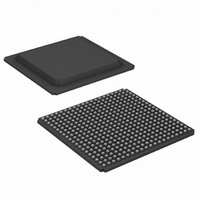
XA3S1600E-4FGG400Q Xilinx Inc, XA3S1600E-4FGG400Q Datasheet - Page 29

XA3S1600E-4FGG400Q
Manufacturer Part Number
XA3S1600E-4FGG400Q
Description
IC FPGA SPARTAN-3E 1600K 400FBGA
Manufacturer
Xilinx Inc
Series
Spartan™-3E XAr
Datasheet
1.XA3S100E-4VQG100I.pdf
(37 pages)
Specifications of XA3S1600E-4FGG400Q
Number Of Logic Elements/cells
33192
Number Of Labs/clbs
3688
Total Ram Bits
663552
Number Of I /o
304
Number Of Gates
1600000
Voltage - Supply
1.14 V ~ 1.26 V
Mounting Type
Surface Mount
Operating Temperature
-40°C ~ 125°C
Package / Case
400-BGA
Package
400FBGA
Family Name
XA SpartanÂ-3E
Device Logic Units
33192
Device System Gates
1600000
Maximum Internal Frequency
572 MHz
Typical Operating Supply Voltage
1.2 V
Maximum Number Of User I/os
304
Ram Bits
663552
Re-programmability Support
Yes
Lead Free Status / RoHS Status
Lead free / RoHS Compliant
Available stocks
Company
Part Number
Manufacturer
Quantity
Price
Company:
Part Number:
XA3S1600E-4FGG400Q
Manufacturer:
XilinxInc
Quantity:
3 000
Company:
Part Number:
XA3S1600E-4FGG400Q
Manufacturer:
Xilinx Inc
Quantity:
10 000
Part Number:
XA3S1600E-4FGG400Q
Manufacturer:
XILINX/赛灵思
Quantity:
20 000
Configuration and JTAG Timing
Table 33: Power-On Timing and the Beginning of Configuration
DS635 (v2.0) September 9, 2009
Product Specification
Notes:
1.
2.
3.
T
T
T
T
T
POR
PROG
PL
INIT
ICCK
(2)
The numbers in this table are based on the operating conditions set forth in
and V
Power-on reset and the clearing of configuration memory occurs during this period.
This specification applies only to the Master Serial, SPI, BPI-Up, and BPI-Down modes.
(2)
Symbol
(3)
CCAUX
R
lines.
The time from the application of V
Bank 2 supply voltage ramps (whichever occurs last) to the
rising transition of the INIT_B pin
The width of the low-going pulse on the PROG_B pin
The time from the rising edge of the PROG_B pin to the
rising transition on the INIT_B pin
Minimum Low pulse width on INIT_B output
The time from the rising edge of the INIT_B pin to the
generation of the configuration clock signal at the CCLK
output pin
Description
CCINT
www.xilinx.com
, V
CCAUX
, and V
Table
CCO
6. This means power must be applied to all V
XA3S100E
XA3S250E
XA3S500E
XA3S1200E
XA3S1600E
All
XA3S100E
XA3S250E
XA3S500E
XA3S1200E
XA3S1600E
All
All
Device
-4 Speed Grade
Min
250
0.5
0.5
-
-
-
-
-
-
-
-
-
-
Max
0.5
0.5
4.0
5
5
5
5
7
1
2
2
-
-
CCINT
Units
, V
ms
ms
ms
ms
ms
ms
ms
ms
ms
ms
μs
ns
μs
CCO
29
,


