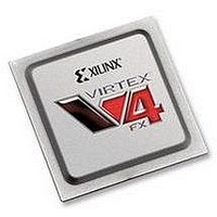
XC4VFX60-10FFG1152C Xilinx Inc, XC4VFX60-10FFG1152C Datasheet - Page 31

XC4VFX60-10FFG1152C
Manufacturer Part Number
XC4VFX60-10FFG1152C
Description
IC FPGA VIRTEX-4 FX 60K 1152FBGA
Manufacturer
Xilinx Inc
Series
Virtex™-4r
Datasheets
1.XC4VFX12-10FFG668C.pdf
(58 pages)
2.XC4VFX12-10FFG668C.pdf
(9 pages)
3.XC4VFX12-10FFG668C.pdf
(406 pages)
Specifications of XC4VFX60-10FFG1152C
Total Ram Bits
4276224
Number Of Logic Elements/cells
56880
Number Of Labs/clbs
6320
Number Of I /o
576
Voltage - Supply
1.14 V ~ 1.26 V
Mounting Type
Surface Mount
Operating Temperature
0°C ~ 85°C
Package / Case
1152-BBGA, FCBGA
No. Of Logic Blocks
6656
No. Of Macrocells
56880
Family Type
Virtex-4
No. Of Speed Grades
10
No. Of I/o's
576
Clock Management
DCM
Core Supply
RoHS Compliant
Package
1152FCBGA
Family Name
Virtex®-4
Device Logic Units
56880
Typical Operating Supply Voltage
1.2 V
Maximum Number Of User I/os
576
Ram Bits
4276224
Lead Free Status / RoHS Status
Lead free / RoHS Compliant
For Use With
HW-V4-ML410-UNI-G - EVALUATION PLATFORM VIRTEX-4
Number Of Gates
-
Lead Free Status / RoHS Status
Lead free / RoHS Compliant
Available stocks
Company
Part Number
Manufacturer
Quantity
Price
Company:
Part Number:
XC4VFX60-10FFG1152C
Manufacturer:
XilinxInc
Quantity:
3 000
Company:
Part Number:
XC4VFX60-10FFG1152C
Manufacturer:
Xilinx Inc
Quantity:
10 000
CLB Switching Characteristics
Table 37: CLB Switching Characteristics
DS302 (v3.7) September 9, 2009
Product Specification
Notes:
1.
2.
3.
4.
Combinatorial Delays
Sequential Delays
Setup and Hold Times of CLB Flip-Flops Before/After Clock CLK
Set/Reset
T
T
T
T
T
T
T
T
T
T
T
T
T
T
T
T
T
T
T
T
T
T
F
A Zero “0” Hold Time listing indicates no hold time or a negative hold time. Negative values cannot be guaranteed “best-case,” but if a “0” is listed,
there is no positive hold time.
The values in this column apply to all XC4VFX -12 parts except XC4VFX12 -12. For XC4VFX12 -12 values, use the values in the adjacent 4VLX/SX
-12 column.
These items are of interest for Carry Chain applications.
XC4VFX -11 devices are 1181 MHz.
ILO
IF5
IF5X
IF6Y
INAFX
INBFX
BXX
BYY
BXCY
BYCY
BYP
OPCYF
OPCYG
CKO
CKLO
DICK
CECK
FXCK
SRCK
CINCK
RPW
RQ
TOG
Symbol
/
/
/
/
T
/
T
T
T
T
CKDI
CKFX
CKCE
CKSR
CKCIN
4-input function: F/G inputs to X/Y outputs
5-input function: F/G inputs to F5 output
5-input function: F/G inputs to X output
FXINA or FXINB inputs to YMUX output
FXINA input to FX output via MUXFX
FXINB input to FX output via MUXFX
BX input to XMUX output
BY input to YMUX output
BX input to C
BY input to C
C
F input to C
G input to C
FF Clock CLK to XQ/YQ outputs
Latch Clock CLK to XQ/YQ outputs
BX/BY inputs
CE input
FXINA/FXINB inputs
SR/BY inputs (synchronous)
C
Minimum Pulse Width, SR/BY inputs
Delay from SR/BY inputs to XQ/YQ outputs
(asynchronous)
Toggle Frequency (MHz) (for export control)
IN
IN
input to C
Data Inputs (DI) – Getting out from carry chain
OUT
OUT
OUT
OUT
OUT
output – Getting out from carry chain
output – Getting out from carry chain
output – Getting into carry chain
output – Getting into carry chain
output – Carry chain delay
Description
www.xilinx.com
Virtex-4 FPGA Data Sheet: DC and Switching Characteristics
(3)
(3)
(3)
(3)
(3)
(3)
XC4VFX
–0.09
–0.16
–0.14
–0.74
–0.23
1181
0.15
0.36
0.44
0.30
0.21
0.21
0.59
0.43
0.60
0.49
0.07
0.45
0.44
0.28
0.37
0.36
0.58
0.42
1.04
0.52
0.54
1.05
(2)
-12
XC4VLX/SX
Speed Grade
–0.09
–0.16
–0.14
–0.73
–0.23
1205
0.15
0.35
0.43
0.30
0.21
0.20
0.58
0.43
0.59
0.48
0.07
0.44
0.43
0.28
0.36
0.36
0.57
0.41
1.02
0.51
0.53
1.03
1205
–0.09
–0.16
–0.14
–0.73
–0.23
0.17
0.40
0.49
0.34
0.23
0.23
0.65
0.48
0.66
0.54
0.08
0.50
0.48
0.31
0.41
0.40
0.64
0.46
1.15
0.57
0.59
1.15
ALL DEVICES
-11
(4)
–0.09
–0.16
–0.14
–0.73
–0.23
1028
0.20
0.46
0.57
0.39
0.27
0.26
0.76
0.56
0.78
0.63
0.09
0.58
0.57
0.36
0.48
0.47
0.75
0.54
1.35
0.67
0.70
1.35
-10
ns, Max
ns, Max
ns, Max
ns, Max
ns, Max
ns, Max
ns, Max
ns, Max
ns, Max
ns, Max
ns, Max
ns, Max
ns, Max
ns, Max
ns, Max
ns, Max
ns, Min
ns, Min
ns, Min
ns, Min
ns, Min
ns, Min
Units
MHz
31


