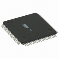
AT40K20-2AQC Atmel, AT40K20-2AQC Datasheet - Page 12

AT40K20-2AQC
Manufacturer Part Number
AT40K20-2AQC
Description
IC FPGA 20K GATES 100TQFP
Manufacturer
Atmel
Series
AT40K/KLVr
Specifications of AT40K20-2AQC
Number Of Logic Elements/cells
1024
Total Ram Bits
8192
Number Of I /o
78
Number Of Gates
30000
Voltage - Supply
4.75 V ~ 5.25 V
Mounting Type
Surface Mount
Operating Temperature
0°C ~ 70°C
Package / Case
100-TFQFP
Lead Free Status / RoHS Status
Contains lead / RoHS non-compliant
Number Of Labs/clbs
-
Other names
AT40K202AQC
Available stocks
Company
Part Number
Manufacturer
Quantity
Price
Company:
Part Number:
AT40K20-2AQC
Manufacturer:
YAGEO
Quantity:
640 000
12
AT40K/AT40KLV Series FPGA
Reading and writing of the 10 ns 32 x 4 dual-port FreeRAM are independent of each
other. Reading the 32 x 4 dual-port RAM is completely asynchronous. Latches are
transparent; when Load is logic 1, data flows through; when Load is logic 0, data is
latched. These latches are used to synchronize Write Address, Write Enable Not, and
Din signals for a synchronous RAM. Each bit in the 32 x 4 dual-port RAM is also a trans-
parent latch. The front-end latch and the memory latch together form an edge-triggered
flip flop. When a nibble (bit = 7) is (Write) addressed and LOAD is logic 1 and WE is
logic 0, data flows through the bit. When a nibble is not (Write) addressed or LOAD is
logic 0 or WE is logic 1, data is latched in the nibble. The two CLOCK muxes are con-
trolled together; they both select CLOCK (for a synchronous RAM) or they both select
“1” (for an asynchronous RAM). CLOCK is obtained from the clock for the sector-column
immediately to the left and immediately above the RAM block. Writing any value to the
RAM clear byte during configuration clears the RAM (see the “ AT40K Configuration
Series” application note at www.atmel.com).
Figure 8. RAM Logic
Figure 9 on page 13 shows an example of a RAM macro constructed using the
AT40K/AT40KLV’s FreeRAM cells. The macro shown is a 128 x 8 dual-ported asyn-
chronous RAM. Note the very small amount of external logic required to complete the
address decoding for the macro. Most of the logic cells (core cells) in the sectors occu-
pied by the RAM will be unused: they can be used for other logic in the design. This
logic can be automatically generated using the macro generators.
WEN
Aout
Ain
Din
5
5
4
“1”
0
1
Latch
Latch
Latch
Load
Load
Load
CLOCK
Read Address
Write Address
Write Enable NOT
Din
RAM-Clear Byte
Dual-port
Clear
1
Load
32 x 4
RAM
“1”
0
Dout
“1”
OE
0896C–FPGA–04/02
4
Dout


