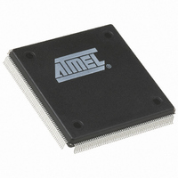
AT40K40LV-3EQC Atmel, AT40K40LV-3EQC Datasheet - Page 12

AT40K40LV-3EQC
Manufacturer Part Number
AT40K40LV-3EQC
Description
IC FPGA 3.3V 2304 CELL 240PQFP
Manufacturer
Atmel
Series
AT40K/KLVr
Datasheet
1.AT40K40LV-3BQC.pdf
(54 pages)
Specifications of AT40K40LV-3EQC
Number Of Logic Elements/cells
2304
Total Ram Bits
18432
Number Of I /o
193
Number Of Gates
50000
Voltage - Supply
3 V ~ 3.6 V
Mounting Type
Surface Mount
Operating Temperature
0°C ~ 70°C
Package / Case
240-BFQFP
Lead Free Status / RoHS Status
Contains lead / RoHS non-compliant
Number Of Labs/clbs
-
Other names
AT40K40LV3EQC
Clocking and Set/Reset
Each of 8 dedicated Global Clock buses is connected to a
dual-use Global Clock pad (GCK1 - GCK8). An internal sig-
nal can be placed on a Global Clock bus by routing that sig-
nal to a Global Clock pad. Each column of the array has a
Column Clock selected from one of the 8 Global Clock
buses. The extreme-left Column Clock mux has two addi-
tional inputs from dual-use pins FCK1 & FCK2 to provide
fast clocking to left-side I/O. The extreme-right Column
Clock mux has two additional inputs from dual-use pins
FCK3 & FCK4 to provide fast clocking to right-side I/O.
Each sector column of 4 cells can be clocked from a (Plane
4) express bus or from the Column Clock. Clocking to the 4
cells can be disabled. The Plane 4 express bus used for
clocking is half length at the array edge. The clock provided
to each sector column of 4 cells can be either inverted or
not inverted. The register in each cell is triggered on a ris-
ing clock edge. On power up, constant “0” is provided to
each registers clock pins.
12
AT40K
A dedicated Global Set/Reset bus can be driven by any
USER I/O pad, except those used for clocking, Global or
Fast. An internal signal can be placed on the Global
Set/Reset bus by routing that signal to the pad pro-
grammed as the Global Set/Reset input. Global Set/Reset
is distributed to each column of the array. Each sector col-
umn of 4 cells can be Set/Reset by a (Plane 5) express bus
or by the Global Set/Reset. The Plane 5 express bus used
for Set/Reset is half length at array edge. The Set/Reset
provided to each sector column of 4 cells can be either
inverted or not inverted. The function of the Set/Reset input
of a register (either Set or Reset) is determined by a config-
uration bit in each cell. The Set/Reset input of a register is
Active Low (logic 0). Setting or resetting of a register is
asynchronous. On power up, a logic 1 (a high) is provided
by each register, i.e., all registers are set at power up.


