20-101-0522 Rabbit Semiconductor, 20-101-0522 Datasheet - Page 83
20-101-0522
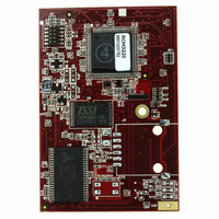
Manufacturer Part Number
20-101-0522
Description
MODULE RABBITCORE RCM3220
Manufacturer
Rabbit Semiconductor
Datasheet
1.20-101-0522.pdf
(96 pages)
Specifications of 20-101-0522
Module/board Type
MPU Core Module
Product
Microcontroller Modules
Core Processor
Rabbit 3000
Clock Speed
44.2 MHz
Interface Type
Ethernet, Serial
Flash
512 KB
Timers
10 x 8 bit, 1 x 10 bit
Operating Supply Voltage
3.15 V to 3.45 V
Board Size
69 mm x 47 mm x 22 mm
Core
RCM3220
Processor Series
RCM3200
For Use With/related Products
RCM3220
Lead Free Status / RoHS Status
Lead free / RoHS Compliant
Other names
316-1098


F.3 Using Parallel Port F
Parallel Port F is a byte-wide port with each bit programmable for data direction and drive.
These are simple inputs and outputs controlled and reported in the Port F Data Register.
As outputs, the bits of the port are buffered, with the data written to the Port F Data Regis-
ter transferred to the output pins on a selected timing edge. The outputs of Timer A1,
Timer B1, or Timer B2 can be used for this function, with each nibble of the port having a
separate select field to control this timing. These inputs and outputs are also used for
access to other peripherals on the chip.
As outputs, Parallel Port F can carry the four Pulse Width Modulator outputs on PF4–PF 7
(J6, pins 5–8). As inputs, Parallel Port F can carry the inputs to the Quadrature Decoders
on PF0–PF3 (J6, pins 1–4). When Serial Port C or Serial Port D is used in clocked serial
mode, two pins of Port F (PF0 / J6:1 and PF1 / J6:2) are used to carry the serial clock sig-
nals. When the internal clock is selected in these serial ports, the corresponding bit of Par-
allel Port F is set as an output.
F.3.1 Parallel Port F Registers
Data Direction Register—
, address 00111111 (0x3F), write-only, default value on
PFDDR
reset 00000000. For each bit position, write a 1 to make the corresponding port line an
output, or 0 to produce an input.
Drive Control Register—PFDCR, address 00111110 (0x3E), Write-only, no default on
reset (port defaults to all inputs). Effective only if the corresponding port bits are set as
outputs, each bit set to 1 configures the corresponding port bit as open drain. Setting the
bit to 0 configures that output as active high or low.
Function Register—PFFR, address 00111101 (0x3D), Write-only, no default on reset.
This register sets the alternate output function assigned to each of the pins of the port.
When set to 0, the corresponding port pin functions normally as an output (if configured to
be an output in PFDDR). When set to 1, each bit sets the corresponding pin to have the
alternate output function as shown in the summary table at the end of this section.
Control Register—PFCR, address 00111100 (0x3C), Write-only, default on reset
xx00xx00. This register sets the transfer clock, which controls the timing of the outputs on
each nibble of the output ports to allow close synchronization with other events. The sum-
mary table at the end of this section shows the settings for this register. The default values
on reset transfer the output values on CLK/2.
Data Register—PFDR, address 00111000 (0x38), Read or Write, no default value on
reset. On read, the current state of the pins is reported. On write, the output buffer is writ-
ten with the value for transfer to the output port register on the next rising edge of the
transfer clock, set in the PFCR.
User’s Manual
79
Related parts for 20-101-0522
Image
Part Number
Description
Manufacturer
Datasheet
Request
R

Part Number:
Description:
COMPUTER SGL-BRD BL2500 29.4MHZ
Manufacturer:
Rabbit Semiconductor
Datasheet:

Part Number:
Description:
COMPUTER SGL-BRD BL2500 29.4MHZ
Manufacturer:
Rabbit Semiconductor
Datasheet:

Part Number:
Description:
DISPLAY GRAPHIC 12KEY PROG OP670
Manufacturer:
Rabbit Semiconductor
Datasheet:
Part Number:
Description:
DISPLAY GRAPHIC 12KEY ETH OP6700
Manufacturer:
Rabbit Semiconductor
Datasheet:

Part Number:
Description:
COMPUTER SINGLE-BOARD BL2030
Manufacturer:
Rabbit Semiconductor
Part Number:
Description:
COMPUTER SGL-BOARD ETH BL2010
Manufacturer:
Rabbit Semiconductor

Part Number:
Description:
MODULE OP6810 W/O ETH/MEM EXPANS
Manufacturer:
Rabbit Semiconductor
Datasheet:
Part Number:
Description:
COMPUTER SINGLE-BOARD BL2020
Manufacturer:
Rabbit Semiconductor
Part Number:
Description:
COMPUTER BL2010 W/FRICTION LOCK
Manufacturer:
Rabbit Semiconductor
Part Number:
Description:
COMPUTER BL2020 W/FRICTION LOCK
Manufacturer:
Rabbit Semiconductor
Part Number:
Description:
COMPUTER SGL-BRD BL2500 44.2MHZ
Manufacturer:
Rabbit Semiconductor
Datasheet:
Part Number:
Description:
COMPUTER SGL-BOARD FULL BL2000
Manufacturer:
Rabbit Semiconductor

Part Number:
Description:
COMPUTER SINGLE-BOARD BL2110
Manufacturer:
Rabbit Semiconductor

Part Number:
Description:
COMPUTER SGL-BRD 29.4MHZ BL2610
Manufacturer:
Rabbit Semiconductor
Datasheet:
Part Number:
Description:
INTERFACE OP6800 512K FLASH&SRAM
Manufacturer:
Rabbit Semiconductor
Datasheet: