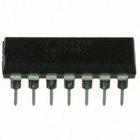
FMS7401LVN14 Fairchild Semiconductor, FMS7401LVN14 Datasheet - Page 10

FMS7401LVN14
Manufacturer Part Number
FMS7401LVN14
Description
IC CTRLR POWER DGTL EEPROM 14DIP
Manufacturer
Fairchild Semiconductor
Datasheet
1.FMS7401LVN.pdf
(81 pages)
Specifications of FMS7401LVN14
Applications
Digital Power Controller
Core Processor
8-Bit
Program Memory Type
EEPROM (1 kB)
Ram Size
64 x 8
Number Of I /o
8
Voltage - Supply
2.7 V ~ 3.6 V
Operating Temperature
-40°C ~ 125°C
Mounting Type
Through Hole
Package / Case
14-DIP (0.300", 7.62mm)
Output Current
5 mA
Input Voltage
2.7 V to 3.6 V
Switching Frequency
2 MHz
Operating Temperature Range
- 40 C to + 125 C
Mounting Style
Through Hole
Lead Free Status / RoHS Status
Lead free / RoHS Compliant
Interface
-
Controller Series
-
Lead Free Status / Rohs Status
Lead free / RoHS Compliant
Other names
FMS7401LVN14_NL
FMS7401LVN14_NL
FMS7401LVN14_NL
FMS7401L
2
The FMS7401L may be clocked using its internal oscillator circuit or using an external digital clock signal. The desired clock
source is selectable by the CMODE bit of the Initialization Register 1.
and the desired clock source (also called the device reference clock or F
defaulted from the factory to use the internal oscillator as their main system instruction clock source. After power-up, the inter-
nal oscillator runs continuously unless entering Halt Mode or using an external clock source.
Table 2. CMODE Bit Definition
The internal oscillator signal is factory trimmed to yield the F
of the datasheet. If the external digital clock is selected, the input signal must have a 50/50 duty cycle, can range from DC to
the F
device should be provided through the AIN3/G1 input.
Once the source of F
the Programmable Comparator circuit, and is divided-by-2 to be used as the main system instruction clock (F
(see
2.1
The FMS7401L has an internal digital clock multiplier (PLL) that steps-up the F
32. The multiplied PLL output is then divided by a factor of 1, 2, 4, and 8 in order to generate its programmable output fre-
quencies that may be used as the main system instruction clock or by the PWM Timer 1 circuit. The PLL provides the ability to
run the PWM Timer 1 circuit at a frequency as high as 64MHz while the rest of the device operates at a much slower frequency
keeping the total current consumption low.
The reference clock of the PLL is defined by the F
signal. In order to yield the proper output frequencies offered by the PLL, F
fied in the
the REFBY2 bit in the ADCNTRL2 register
quency of the F
grammable Comparator circuit operates at a F
must be supplied at the specified F
Table 3. PLL Frequency Selection (F
The PLL outputs may be used to clock both the PWM Timer 1 circuit and the main system clock. However, the PLL must first
be enabled by setting the PLLEN bit of the PSCALE register.
Before using any of the PLL outputs, software must wait the T
quency and in phase. The PLLEN bit may not be changed while the PWM Timer 1 circuit is in run mode.
to this bit during this condition will not change its value.
The PWM Timer 1 circuit may be clocked either by the PLL’s F
bit of the PSCALE register
not be set if the PLL is not enabled (PLLEN=0) or changed while the PWM Timer 1 circuit is in run mode.
to this bit during these conditions will not change its value.
10
CMODE
0
0
1
1
Figure 3
FS[1:0]
OSC
0
1
Clock Circuit
PLL
, and must be available upon power-up. When the device is driven using an external clock source, the clock input to the
Electrical Characteristics
0
1
0
1
and
RCLK2
Figure
RCLK1
signal. Once the REFBY2 bit is set, the F
External digital clock (G1/AIN3)
F
2 MHz
2 MHz
2 MHz
2 MHz
Internal Oscillator (@ F
RCLK2
4).
F
is selected, the clock is then used as the reference clock for the PLL, the clock to the digital filter in
4
RCLK1
selects between the PLL’s F
Clock Source
OSC
section of the datasheet. In the case that F
frequency in order to meet the specified F
(FMODE = 0)
PLL
3
OSC
1 MHz
1 MHz
1 MHz
1 MHz
RCLK1
must be set in order to divide the F
F
/F
ICLK
)
OSC
RCLK2
/2 frequency. If an external digital clock is sourcing F
= 2MHz)
PWMCLK
signal (as shown in
OSC
4
PLL_LOCK
Once set, the PLL is turned on and begins the locking phase.
RCLK2
PWMCLK
output (if FSEL=1) or F
frequency as specified in the
(FMODE = 1)
8 MHz
8 MHz
8 MHz
8 MHz
signal that drives the PLL and digital filter in the Pro-
F
1
ICLK
to ensure that the PLL is locked into its appropriate fre-
During the reset sequence, the CMODE bit is updated
output or by the main system clock (F
RCLK1
RCLK2
Figure 3
) takes control of the device. All devices are
RCLK1
PLL
RCLK1
RCLK1
must operate at the F
frequency of the F
is operating at the upper F
and
by 2 to yield the appropriate F
frequency by a multiplication factor of
ICLK
Figure
F
16 MHz
32 MHz
64 MHz
8 MHz
PWMCLK
(if FSEL=0). The FSEL bit may
Electrical Characteristics
4) and sourced by the F
PRODUCT SPECIFICATION
RCLK2
PLL
RCLK1
5
5
frequency as speci-
Any write attempts
Any write attempts
REV. 1.0.3 1/24/05
ICLK
signal.
, the input signal
ICLK
OSC
) of the device
). The FSEL
frequency,
PLL
section
RCLK1
fre-
2


