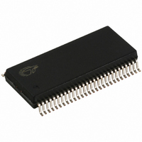
CY7C66113C-PVXC Cypress Semiconductor Corp, CY7C66113C-PVXC Datasheet - Page 25

CY7C66113C-PVXC
Manufacturer Part Number
CY7C66113C-PVXC
Description
IC MCU 8K USB HUB 4 PORT 56TSSOP
Manufacturer
Cypress Semiconductor Corp
Specifications of CY7C66113C-PVXC
Applications
USB Hub/Microcontroller
Core Processor
M8
Program Memory Type
OTP (8 kB)
Controller Series
USB Hub
Ram Size
256 x 8
Interface
I²C, USB, HAPI
Number Of I /o
31
Voltage - Supply
4 V ~ 5.5 V
Operating Temperature
0°C ~ 70°C
Mounting Type
Surface Mount
Package / Case
56-SSOP
No. Of I/o's
31
Eeprom Memory Size
8KB
Ram Memory Size
256Byte
Cpu Speed
48MHz
Digital Ic Case Style
SSOP
Supply
RoHS Compliant
Core Size
8bit
Program Memory Size
8KB
Oscillator Type
External, Internal
Peripherals
DAC
Rohs Compliant
Yes
Controller Family/series
(8051) USB
Embedded Interface Type
HAPI, I2C, USB
Processor Series
CY7C66xx
Core
M8
Data Bus Width
16 bit
Data Ram Size
256 B
Interface Type
HAPI, I2C, USB
Maximum Clock Frequency
12 MHz
Number Of Programmable I/os
39
Number Of Timers
1
Maximum Operating Temperature
+ 70 C
Mounting Style
SMD/SMT
Development Tools By Supplier
CY3654, CY3654-P03
Minimum Operating Temperature
0 C
Lead Free Status / RoHS Status
Lead free / RoHS Compliant
For Use With
CY3649 - PROGRAMMER HI-LO USB M8428-1339 - KIT LOW SPEED PERSONALITY BOARD
Lead Free Status / Rohs Status
Details
Other names
428-1808
Available stocks
Company
Part Number
Manufacturer
Quantity
Price
Company:
Part Number:
CY7C66113C-PVXC
Manufacturer:
HITTITE
Quantity:
101
Part Number:
CY7C66113C-PVXC
Manufacturer:
CIRRUS
Quantity:
20 000
Hardware Assisted Parallel Interface (HAPI)
The CY7C66x13C processor provides a hardware assisted parallel interface for bus widths of 8, 16, or 24 bits, to accommodate data
transfer with an external microcontroller or similar device. Control bits for selecting the byte width are in the HAPI and I
Register
Signals are provided on Port 2 to control the HAPI interface.
and I
overridden. The Port 2 output pins are in CMOS output mode and Port 2 input pins are in input mode (open drain mode with Q3 OFF
in
Table 10. Port 2 Pin and HAPI Configuration Bit Definitions
HAPI Read by External Device from CY7C66x13C
In this case (see
ports. If 16-bit or 24-bit transfers are being made, Port 0 is written
last, because writes to Port 0 asserts the Data Ready bit and the
DReadyPin to signal the external device that data is available.
The external device then drives the OE and CS pins active
(LOW), which causes the HAPI data to be output on the port pins.
When OE is returned HIGH (inactive), the HAPI/GPIO interrupt
is generated. At that point, firmware is reload the HAPI latches
for the next output, again writing Port 0 last.
The Data Ready bit reads the opposite state from the external
DReadyPin on pin P2[3]. If the DRDY Polarity bit is 0, DReadyPin
is active HIGH, and the Data Ready bit is active LOW.
Document Number: 38-08024 Rev. *D
Pin
P2[2]
P2[3]
P2[4]
P2[5]
P2[6]
2
3
4
5
Bit
Figure
2
C Configuration Register. Enabling HAPI causes the GPIO setting in the GPIO Configuration Register
(Figure
7).
Name
LatEmptyPin
DReadyPin
STB
OE
CS
Data Ready
Latch Empty
DRDY Polarity
LEMPTY Polarity
Name
25), bits 1 and 0.
Figure
50), firmware writes data to the GPIO
Direction
Out
Out
In
In
In
R
R
R/W
R/W
R/W
Description (Port 2 Pin)
Ready for more input data from external interface.
Output data ready for external interface.
Strobe signal for latching incoming data.
Output Enable, causes chip to output data.
Chip Select (Gates STB and OE).
Description (HAPI and I
Asserted after firmware writes data to Port 0, until OE driven LOW.
Asserted after firmware reads data from Port 0, until STB driven LOW.
Determines polarity of Data Ready bit and DReadyPin:
If 0, Data Ready is active LOW, DReadyPin is active HIGH.
If 1, Data Ready is active HIGH, DReadyPin is active LOW.
Determines polarity of Latch Empty bit and LatEmptyPin:
If 0, Latch Empty is active LOW, LatEmptyPin is active HIGH.
If 1, Latch Empty is active HIGH, LatEmptyPin is active LOW.
Table 10
HAPI Write by External Device to CY7C66x13C
In this case (see
and CS pins active (LOW) when it drives new data onto the port
pins. When this happens, the internal latches become full, which
causes the Latch Empty bit to be deasserted. When STB is
returned HIGH (inactive), the HAPI and GPIO interrupt is
generated. Firmware then reads the parallel ports to empty the
HAPI latches. If 16-bit or 24-bit transfers are being made, Port 0
should be read last because reads from Port 0 assert the Latch
Empty bit and the LatEmptyPin to signal the external device for
more data.
The Latch Empty bit reads the opposite state from the external
LatEmptyPin on pin P2[2]. If the LEMPTY Polarity bit is 0,
LatEmptyPin is active HIGH, and the Latch Empty bit is active
LOW.
describes these signals and the HAPI control bits in the HAPI
2
C Configuration Register)
Figure
CY7C66013C, CY7C66113C
52), the external device drives the STB
(Figure
2
C Configuration
Page 25 of 59
10) to be
[+] Feedback


