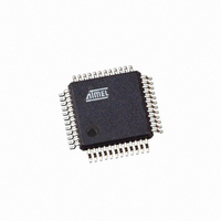
AT43USB326-AC Atmel, AT43USB326-AC Datasheet
AT43USB326-AC
Specifications of AT43USB326-AC
Available stocks


Related parts for AT43USB326-AC


AT43USB326-AC Summary of contents
Page 1
... Furthermore, the AT43USB326 features an on-chip 16-Kbyte program memory and 512 bytes of data memory supported by a standard set of peripherals such as timer/counter modules, watchdog timer and internal and external interrupt sources. The major peripheral included in the AT43USB326 is the USB Hub with an embedded keyboard controller function. Multimedia ...
Page 2
... Pin Configuration Figure 1. AT43USB326 48-lead LQFP AT43USB326 2 PC0 37 PD0 38 PD1 39 VSS2 40 CEXT2 41 DP3 42 AT43USB326 DM3 43 DP2 44 45 DM2 DP0 46 DM0 47 48 RESETN PA5 24 23 PA6 22 PA7 PB0 21 20 PB1 19 PB2 18 PB3 17 PB4 16 PB5 15 PB6 14 PB7 13 PE0 3313D–USB–04/06 ...
Page 3
... Type Pin# Input Output Input Output Bi-directional Bi-directional Bi-directional Bi-directional Bi-directional Bi-directional Bi-directional Bi-directional Bi-directional Bi-directional Bi-directional Bi-directional Bi-directional Bi-directional Bi-directional Bi-directional Bi-directional AT43USB326 Signal 25 PA4/CL4 Bi-directional 26 PA3/CL3 Bi-directional 27 PA2/CL2 Bi-directional 28 PA1/CL1 Bi-directional 29 PA0/CL0 Bi-directional 30 PC7/ROW7 Bi-directional 31 PC6/ROW6 Bi-directional 32 ...
Page 4
... Bi-directional PE[4:7] Bi-directional TEST Input RESETN Input AT43USB326 4 Function 5V Digital Power Supply Ground External Capacitors for Power Supplies – High quality 2.2 µF capacitors must be connected to CEXT1 and 2 for proper operation of the chip. Oscillator Input – Input to the inverting oscillator amplifier. ...
Page 5
... Figure 2. The AT43USB326 Enhanced RISC Architecture with USB Keyboard Controller and Hub Program Memory Instruction Register Instruction Decoder Control Lines 3313D–USB–04/06 Program Status and Counter Control General-purpose Registers ALU 512 x 8 SRAM 2 GPIO Lines USB Hub and Function AT43USB326 ...
Page 6
... USB Hub with attached function The embedded USB hardware of the AT43USB326 is a compound device, consisting port hub with a permanently attached function on one port. The hub and attached function are two independent USB devices, each having its own device addresses and control endpoints. ...
Page 7
... SUBI, CPI, ANDI, and ORI between a constant and a register, and the LDI instruction for load 3313D–USB–04/06 Address Comment $00 $01 $02 $0D $0E $0F $10 $11 $1A X-register low byte $1B X-register high byte $1C Y-register low byte $1D Y-register high byte $1E Z-register low byte $1F Z-register high byte AT43USB326 7 ...
Page 8
... Program Memory The AT43USB326 contains 16K bytes on-chip masked programmable ROM. Since all instruc- tions are 16- or 32-bit words, the program memory is organized 16. The AT43USB326 Program Counter (PC bits wide, thus addressing the 8,192 program memory addresses. Constant tables can be allocated within the entire program memory address space (see the LPM - Load Program Memory instruction description) ...
Page 9
... SRAM Data Table 3 summarizes how the AT43USB326 SRAM Memory is organized. The lower 608 Data Memory Memory locations address the Register file, the I/O Memory and the internal data SRAM. The first 96 locations address the Register File + I/O Memory, and the next 512 locations address the internal data SRAM ...
Page 10
... Table 2. SRAM Organization AT43USB326 10 Register File R0 R1 R30 R31 I/O Registers $00 $01 $3E $3F Data Address Space $0000 $0001 $001E $001F $0020 $0021 $005E $005F Internal SRAM $0060 $0061 $025E $045F USB Registers $1F00 $1FFE $1FFF 3313D–USB–04/06 ...
Page 11
... Function Endpoint 1 Byte Count Register FBYTE_CNT2 Function Endpoint 2 Byte Count Register HSTR Hub Status Register HPCON Hub Port Control Register HPSTAT3 Hub Port 3 Status Register HPSTAT2 Hub Port 2 Status Register HPSTAT1 Hub Port 1 Status Register HPSCR3 Hub Port 3 Status Change Register AT43USB326 11 ...
Page 12
... Table 3. USB Hub and Function Registers (Continued) Address $1FB1 $1FB0 $1FAA $1FA9 $1FA7 $1FA5 $1FA4 $1FA3 AT43USB326 12 Name Function HPSCR2 Hub Port 2 Status Change Register HPSCR1 Hub Port 1 Status Change Register PSTATE3 Hub Port 3 Bus State Register PSTATE2 Hub Port 2 Bus State Register ...
Page 13
... FORCE STALL TX PACKET READY STALL_SENT-ACK FORCE STALL TX PACKET READY STALL_SENT-ACK FORCE STALL TX PACKET READY STALL_SENT-ACK FORCE STALL TX PACKET READY STALL_SENT-ACK AT43USB326 Bit 2 Bit 1 Bit 0 RMWUPE CONFG HADD EN FRWUP RSM GLB SUSP FRWUP IE RSM IE GLB SUSP IE FRWUP MSK RSM MSK ...
Page 14
... All AT43USB326 I/O and peripherals, except for the USB hardware registers, are placed in the I/O space. The I/O locations are accessed by the IN and OUT instructions transferring data between the 32 general-purpose working registers and the I/O space. I/O registers within the address range $00 – ...
Page 15
... USB Hub A block diagram of the USB hardware of the AT43USB326 is shown in Figure 3. The USB hub of the AT43USB326 has 3 downstream ports. The embedded function is permanently attached to Port 1. Ports 2 and 3 are available as external ports. The actual number of ports used is strictly defined by the firmware of the AT43USB326 and can vary from Because the exact configuration is defined by firmware, ports 2 and 3 may even function as permanently attached ports as long as the Hub Descriptor identifies them as such ...
Page 16
... Figure 3. USB Hardware AT43USB326 16 Port 0 XCVR Hub Repeater Serial Interface Engine Port 1 Hub Function Interface Interface Unit Unit AVR Microcontroller Port 2 XCVR Port 3 XCVR Data Address Control 3313D–USB–04/06 ...
Page 17
... V the chip through the CEXT1 and CEXT2 pins. I/O Pin The I/O pins of the AT43USB326 should not be directly connected to voltages less than V more than the voltage at the CEXT pins necessary to violate this rule, insert a series Characteristics resistor between the I/O pin and the source of the external signal source that limits the current into the I/O pin to less than 2 mA ...
Page 18
... Figure 4. Oscillator and PLL Reset and The AT43USB326 provides 12 different interrupt sources with 4 separate reset vectors, each with a separate program vector in the program memory space. Nine of the interrupt sources Interrupt Handling share 2 interrupt reset vectors. These nine are the USB related interrupts. All interrupts are assigned individual enable bits which must be set (one) together with the I-bit in the status reg- ister in order to enable the interrupt ...
Page 19
... Labels Code jmp RESET jmp EXT_INT0 jmp TIM0_OVF jmp USB_HW MAIN: ldi r16, high (RAMEND) out SPH, r16 ldi r16, low (RAMEND) out SPL, r16 <instr> xxx ... ... ... AT43USB326 Comments ; Reset Handler ; IRQ0 Handler ; Timer0 ; USB Handler ; Main Program 19 ...
Page 20
... USB Reset – The AT43USB326 has a feature to separate the USB and microcontroller resets. This feature is enabled by setting the BUS INT EN, bit 3 of the SPRSIE register. A USB bus reset is defined as a SE0 (single ended zero least 4 slow speed USB clock cycles received by Port0 ...
Page 21
... Power-on Reset period can be extended. 3313D–USB–04/06 USB Reset OR Cntr Reset 14-bit Cntr Time-out 1.1 ms 16.0 ms has reached the power-on threshold voltage, regardless of the V CC AT43USB326 ON S FSTRT R Number of WDT cycles 1K 16K directly or via an CC has been applied, the CC CC ...
Page 22
... TIME-OUT INTERNAL RESET Non-USB Related The AT43USB326 has two non-USB 8-bit Interrupt Mask control registers; GIMSK (General Interrupt Mask Register) and TIMSK (Timer/Counter Interrupt Mask Register). Interrupt Handling When an interrupt occurs, the Global Interrupt Enable I-bit is cleared (zero) and all interrupts are disabled ...
Page 23
... Note that external level interrupt does not have a flag, and will only be remembered for as long as the interrupt condition is active. 3313D–USB–04/06 AT43USB326 23 ...
Page 24
... Request 0 is executed from program memory address $002. See also “External Interrupts” on page 26. • Bits 5..0 – Res: Reserved Bits These bits are reserved bits in the AT43USB326 and always read as zero. General Interrupt Flag Register – GIFR Bit $3A ($5A) ...
Page 25
... Timer/Counter0 Overflow interrupt is enabled. The corresponding interrupt (at vector $007) is executed if an overflow in Timer/Counter0 occurs, i.e., when the TOV0 bit is set in the TIFR. • Bit 0 – Res: Reserved Bit This bit is a reserved bit in the AT43USB326 and always reads zero. Timer/Counter Interrupt Flag Register – TIFR $38 ($58) ...
Page 26
... External Interrupts While in the suspend state, the depression of any key will trigger a resume interrupt. This is the only available external interrupt in the AT43USB326. Interrupt The interrupt execution response for all the enabled AVR interrupts is 4 clock cycles minimum. Response Time 4 clock cycles after the interrupt flag has been set, the program vector address for the actual interrupt handling routine is executed ...
Page 27
... This bit selects between the two available sleep modes. When SM is cleared (zero), Idle Mode is selected as Sleep Mode. When SM is set (1), Power Down mode is selected as sleep mode. The AT43USB326 does not support the Idle Mode and SM should always be set to one when entering the Sleep Mode. ...
Page 28
... The Suspend and Resume interrupts are cleared by writing the particular interrupt bit. All other interrupts are cleared when the microcontroller sets a bit in an interrupt acknowledge register. AT43USB326 28 Description Whenever USB hardware decodes a valid Start of Frame. The frame number is stored in the two Frame Number Registers ...
Page 29
... TX Packet Ready is cleared AND TX Complete is set (control and IN endpoints SETUP is set (control endpoints only Complete is set 3313D–USB–04/ SOF INT EOF2 INT – – AT43USB326 Endpoint type CONTROL, OUT CONTROL, IN CONTROL, IN CONTROL HEP0 INT FE2 INT FE1 INT FE0 INT ...
Page 30
... When the FE2 IMSK bit is set (1), the Function Endpoint 2 Interrupt is masked. • Bit 1 – FEP1 IMSK: Enable Endpoint 1 Interrupt When the FE1 IMSK bit is set (1), the Function Endpoint 1 Interrupt is masked. • Bit 0 – FEP0 IMSK: Enable Endpoint 0 Interrupt When the FE0 IMSK bit is set (1), the Function Endpoint 0 Interrupt is masked. AT43USB326 ...
Page 31
... The microcontroller firmware writes this bit to clear the FEP1 bit. • Bit 0 – FEP0 INTACK: Function Endpoint 0 Interrupt Acknowledge The microcontroller firmware writes this bit to clear the FEP0 INT bit. 3313D–USB–04/ SOF INTACK EOF2 INTACK – – AT43USB326 HEP0 INTACK FEP2 IMSK FEP1 INTACK FEP0 INTACK UIAR 31 ...
Page 32
... Port 1. An interrupt is generated if the RSM IE bit of the SPRSIE register is set. • Bit 0 – GLB SUSP: Global Suspend The USB hardware sets this bit when a USB global suspend signaling is detected. An interrupt is generated if the GLBSUSP IE bit of the SPRSIE register is set. AT43USB326 ...
Page 33
... Bit 1 – RSM MSK: Resume Interrupt Mask • Bit 0 – GLB SUSP MSK: Global Suspend Interrupt Enable 3313D–USB–04/ – – – – – – – – AT43USB326 – FRWUP RSM GLB SUSP – FRWUP MSK RSM GLB SUSP SPRSIE SPRSMSK 33 ...
Page 34
... The carry flag C indicates a carry in an arithmetic or logic operation. See the Instruction Set Description for detailed information. Note that the status register is not automatically stored when entering an interrupt routine and restored when returning from an interrupt routine. This must be handled by software. AT43USB326 ...
Page 35
... Note that when a level triggered interrupt is used for wake-up from power down, the low level must be held for a time longer than the reset delay time-out period t will fail to wake up. 3313D–USB–04/06 Bit SP7 SP6 SP5 R/W R/W R/W R/W R/W R AT43USB326 SP4 SP3 SP2 SP1 R/W R/W R/W R/W R/W R/W R/W R ...
Page 36
... Timer/Counter The AT43USB326 provides one general-purpose 8-bit Timer/Counter (T/C). The Timer/Counter has prescaling selection from a 10-bit prescaling timer. The Timer/Counter can either be used as a timer with an internal clock timebase counter with an external pin connection which triggers the counting. Timer/Counter The four different prescaled selections are: CK/8, CK/64, CK/256 and CK/1024 where CK is the oscillator clock ...
Page 37
... Timer/Counter0 useful for lower speed functions or exact timing functions with infrequent actions. Figure 10. Timer/Counter0 Block Diagram Timer Int. Mask Register (TIMSK) 7 Timer/Counter0 (TCNT0) 3313D–USB–04/06 T/C0 Overflow IRQ Timer Int. Flag Register (TIFR) 0 T/C Clock Source AT43USB326 T/C0 Control Register (TCCR0) CK Control Logic T0 37 ...
Page 38
... Timer/Counter0 – TCNT0 Bit $32 ($52) Read/Write Initial Value The Timer/Counter0 is realized as an up-counter with read and write access. If the Timer/Counter0 is written and a clock source is present, the Timer/Counter0 continues count- ing in the clock cycle following the write operation. AT43USB326 – – – ...
Page 39
... Initial Value • Bits 7..5 – Res: Reserved Bits These bits are reserved bits in the AT43USB326 and will always read as zero. • Bit 4 – WDTOE: Watch Dog Turn-Off Enable This bit must be set (one) when the WDE bit is cleared. Otherwise, the watchdog will not be disabled ...
Page 40
... PE[4:7] have 5V tolerant outputs and each has a built-in series resistor of 330Ω nominal value. These output pins are designed for driving an LED connected to the 5V supply. The dedicated functions are summarized in Table 12. Table 12. GPIO Function Assignments Function Scan out[0:7] Scan out[8:15] Scan out[16,17] Scan in[0:7] LED drivers AT43USB326 40 WDP1 WDP0 Number of WDT Oscillator cycles cycles 0 1 ...
Page 41
... PORTA7 PORTA6 PORTA5 PORTA4 R/W R/W R/W R DDA7 DDA6 DDA5 DDA4 R/W R/W R/W R PINA7 PINA6 PINA5 PINA4 N/A N/A N/A N/A AT43USB326 PORTA3 PORTA2 PORTA1 PORTA0 R/W R/W R/W R DDA3 DDA2 DDA1 DDA0 R/W R/W R/W R PINA3 PINA2 PINA1 PINA0 ...
Page 42
... Initial Value The Port B Input Pins address (PINB) is not a register, and this address enables access to the physical value on each Port B pin. When reading PORTB, the Port B Data Latch is read, and when reading PINB, the logical values present on the pins are read. AT43USB326 ...
Page 43
... PORTC7 PORTC6 PORTC5 PORTC4 R/W R/W R/W R DDC7 DDC6 DDC5 DDC4 R/W R/W R/W R PINC7 PINC6 PINC5 PINC4 N/A N/A N/A N/A AT43USB326 PORTC3 PORTC2 PORTC1 PORTC0 R/W R/W R/W R DDC3 DDC2 DDC1 DDC0 R/W R/W R/W R PINC3 PINC2 PINC1 PINC0 ...
Page 44
... Initial Value The Port D Input Pins address (PIND) is not a register, and this address enables access to the physical value on each Port D pin. When reading PORTD, the Port D Data Latch is read, and when reading PIND, the logical values present on the pins are read. AT43USB326 ...
Page 45
... PORTE7 PORTE6 PORTE5 PORTE4 R/W R/W R/W R DDE7 DDE6 DDE5 DDE4 R/W R/W R/W R PINE7 PINE6 PINE5 PINE4 R/W R/W R/W R/W N/A N/A N/A N/A AT43USB326 – – PORTE1 PORTE0 – – DDE1 DDE0 R R R/W R – – PINE1 PINE0 ...
Page 46
... CPU. It initiates interrupts and acts upon commands sent by the firmware. The USB function hardware of the AT43USB326 makes the physical interface and the proto- col layer transparent to the user. To start the process, the firmware must first enable the endpoints and which place them in receive mode by default ...
Page 47
... ANY STABLE STATE RX_SETUP_INT Setup Response RX_OUT_INT TX_COMPLETE_INT Control Write Data Response RX_OUT_INT TX_COMPLETE_INT TX_COMPLETE_INT Control Control Write Status Read Status Response Response Idle AT43USB326 Data Status Stage Stage … OUT(0) OUT(0/1) IN(1) IN(1) DATA0 DATA0/1 DATA1(0) IN(0) … IN(0/1) OUT(1) DATA0 DATA0/1 ...
Page 48
... The following information describes how the AT43USB326’s USB hardware and firmware operates during a control transfer between the host and the hub’s or function’s control endpoint. Legend: Idle State This is the default state from power-up. Setup Response State The Function Interface Unit (FIU) receives a SETUP token with 8 bytes of data from the Host. ...
Page 49
... Hardware Hardware DATA0/DATA1 Packet Ready = 0, send NAK Set TX Complete → INT Repeat steps 1 through 8 AT43USB326 Firmware 5. Read UISR 6. Read CSR0 7. If SET ADDRESS, program the new Address, set ADD_EN bit 8. Clear TX_COMPLETE, clear Data End, set Force STALL in CAR0 9 ...
Page 50
... FIU places the incoming data into the FIFO, issues an ACK to the host, and asserts an RX_OUT interrupt. 1. OUT token from Host 2. Put DATA0/DATA1 into FIFO 3. ACK to Host 4. Set RX OUT → INT AT43USB326 50 Hardware 4. Read UISR 5. Read CSR0 6. Clear RX OUT, set Data End, set Force Stall in H/FCAR0 ...
Page 51
... TX_COMPLETE interrupt token from Host 2. Send Data1(0) 3. ACK from Host 4. Set TX Complete → INT 3313D–USB–04/06 Hardware 5. Read UISR 6. Read CSR0 7. Clear TX COMPLETE, clear Data 8. Set UIAR[EP0 INTACK] to clear the AT43USB326 Firmware End, set Force STALL in CAR0 interrupt source 51 ...
Page 52
... FIU places the incoming data into the FIFO, issues an ACK to the host, and asserts an RX_OUT interrupt. 1. Read UISR 2. Read FCSR1/2 3. Read FIFO 4. Clear RX_OUT If more data: Wait for RX_OUT interrupt If no more data: set DATA END 5. Set UIAR[FEP1/2 INTACK] to clear the interrupt source AT43USB326 52 3313D–USB–04/06 ...
Page 53
... Initial Value • Bit 7 – SAEN: Single Address Enable The Single Address Enable bit allows the microcontroller to configure the AT43USB326 into a single address or a composite device. Once this capability is enabled, the hub endpoint 0 (HEP0) is converted from a control endpoint to a programmable function endpoint FEP3; all the endpoints would then operate on the single address. • ...
Page 54
... Disable endpoint 1 = Enable endpoint • Bit 6..4 – Reserved These bits are reserved in the AT43USB326 and will read as zero. • Bit 3 – DTGLE: Data Toggle Identifies DATA0 or DATA1 packets. This bit will automatically toggle and requires clearing by the firmware only in certain special circumstances. ...
Page 55
... Disable endpoint 1 = Enable endpoint • Bit 6..4 – Reserved These bits are reserved in the AT43USB326 and will read as zero. • Bit 3 – DTGLE: Data Toggle Identifies DATA0 or DATA1 packets. This bit will automatically toggle and requires clearing by the firmware only in certain special circumstances. ...
Page 56
... Read/Write Initial Value • Bit 7...4 – Reserved These bits are reserved in the AT43USB326 and will read as zero. • Bit 3 – P3 SC: Port 3 Status Change • Bit 2 – P2 SC: Port 2 Status Change • Bit 1 – P1 SC: Port 1 Status Change • Bit 0 – H SC: Hub Status Change ...
Page 57
... USB Hub and Function endpoints. This count includes the 16-bit CRC. To get the actual byte count of the data, subtract the count in the register by 2. The maximum byte count supported by the AT43USB326 is 8 bytes. Hub endpoint 1 has no byte count register. Hub EP0 $1FCF ...
Page 58
... Read/Write Initial Value • Bit 7..4 – Reserved These bits are reserved in the AT43USB326 and will read as zero. • Bit 3 – STALL SENT The USB hardware sets this bit after a STALL has been sent to the host. The firmware uses this bit when responding to a Get Status[Endpoint] request read only bit and that is cleared indirectly by writing a one to the STALL_SENT_ACK bit of the Control and Acknowl- edge Register ...
Page 59
... TX DATA FORCE DIR PACKET END STALL READY TX DATA FORCE DIR PACKET END STALL READY R/W R/W R/W R AT43USB326 STALL_ RX_ RX_OUT_ TX_ SENT_ SETUP_ PACKET_ COMPLETE_ ACK ACK ACK ACK STALL_ RX_ RX_OUT_ TX_ SENT_ SETUP_ PACKET_ COMPLETE_ ACK ACK ACK ...
Page 60
... Read/Write Initial Value • Bit 7..4 – Reserved These bits are reserved in the AT43USB326 and will read as zero. • Bit 3 – STALL SENT The USB hardware sets this bit after a STALL has been sent to the host. The firmware uses this bit when responding to a Get Status[Endpoint] request read only bit and that is cleared indirectly by writing a one to the STALL_SENT_ACK bit of the Control and Acknowl- edge Register ...
Page 61
... Read/Write Initial Value • Bit 7 – Reserved This bit is reserved in the AT43USB326 and will read as zero. • Bit 6 – DATA END When set firmware, this bit indicate that the microcontroller has either placed the last data packet in FIFO, or that the microcontroller has processed the last data packet it expects from the Host. • ...
Page 62
... Controlling each port per host command The first two tasks of the hub are similar to that of a USB function and are described in detail in the following section. The descriptions will cover the features of the AT43USB326's hub and how to program it to make a USB-compliant hub. ...
Page 63
... Initial Value • Bit 7...5 – Reserved Bits These bits are reserved in the AT43USB326 and will read as zeros. • Bit 4 – SUSP FLG: Suspend Flag This bit is set to 1 while the USB hardware is in the suspended state. This bit is a firmware read only bit set and cleared by the USB hardware. • ...
Page 64
... Hub Status Register In the AT43USB326 overcurrent detection and port power switch control output processing is done in firmware. The hardware is designed so that various types of hubs are possible just through firmware modifications. 1. Hub local power status, bits 0 and 2, are optional features and apply to hubs that report on a global basis ...
Page 65
... Read/Write Initial Value • Bit 7 – Reserved This bits is reserved in the AT43USB326 and will read as zero. • Bit 6..4 – HPCON2..0: Hub Port Control Command These bits are written by firmware to control the port states upon receipt of a Host request. Disable Port = ClearPortFeature(PORT_ENABLE) Action: USB hardware places addressed port in disabled state ...
Page 66
... These bits define which port is being addressed for the command defined by bits [2:0]. AT43USB326 66 Bit2 Bit1 Bit0 Port addresses 1 Port3 0 Port2 3313D–USB–04/06 ...
Page 67
... The ports can also exit from the suspended state through a remote wakeup if this feature is enabled. For Ports 2:3, this means detection of a connect/disconnect or an upstream directed signaling. Remote wakeup for the embedded function is initiated through an external interrupt at INT0. 3313D–USB–04/06 AT43USB326 67 ...
Page 68
... Port3 $1FBA Read/Write Initial Value • Bit 7 – Reserved This bit is reserved in the AT43USB326 and will read as zero. • Bit 6 – LSP: Low-speed Device Attached 0 = Full-speed device attached to this port 1 = Slow-speed device attached to this port Set to 0 for Port 1 (full-speed only). Set and cleared by the hardware upon detection of device at EOF2. • ...
Page 69
... These registers contain the state of the ports’ DP and DM pins, which will be sent to the host upon receipt of a GetBusState request. • Bit 7..2 – Reserved These bits are reserved in the AT43USB326 and will read as zero. • Bit 1 – DPSTATE: DPlus State Value last EOF. Set and cleared by hardware at EOF2. ...
Page 70
... Except for bit 3, the Port Overcurrent Indicator Change, the bits in this register are set by the USB hardware. Otherwise, the firmware should only clear these bits. • Bit 7..5 – Reserved These bits are reserved in the AT43USB326 and will read as zero. • Bit 4 – RSTSC: Port Reset Status Change change ...
Page 71
... The embedded hub in a keyboard will most likely be a bus-powered hub even though the hard- Management ware of the AT43USB326 is designed to accommodate both types of hubs. Management of the downstream port power is also defined by the firmware: per port or global overcurrent sensing, individual or gang power switching. While the interface to the external power supply monitoring and switching is achieved through the microcontroller’ ...
Page 72
... Figure 12 shows a simplified diagram of a power management circuit of an AT43USB326 based hub design with global overcurrent protection and ganged power switching for the two external downstream ports. The over-current protection and port power switching for the AT43USB326 is best imple- mented in the so-called multiple gang. The Hub Characteristic’s bits in the Hub Descriptor are set as follows: • ...
Page 73
... As part of the ISR, the firmware clears the GLB_SUSP bit. Remote Wakeup While the AT43USB326 is in global suspend, resume signaling is also possible through remote wakeup if the remote wakeup feature is enabled. Remote wakeup is defined as a port connect, port disconnect or resume signaling received at a downstream port or, in case of the embedded function, through an external interrupt ...
Page 74
... Embedded Function hardware enables the oscillator and asserts the RSM and FRWUP interrupts. 2. Propagate resume signaling 3. Enable Oscillator 4. Set RSM and FRMWUP bits → interrupt AT43USB326 74 Hardware 1.Host resumes signaling 6. Reset RSM and GBL SUSP bits 7. Restore GPIO states if required 8. Clear UOVCER bit 2 9 ...
Page 75
... Selective Resume, Embedded Function 6. Send updated port status at next 3313D–USB–04/06 Hardware command Hardware Hardware IN to endpoint1 AT43USB326 Firmware 1. Set or Clear Port Feature PORT_SUSPEND decoded 2. Write HPCON[2:0] and HPADD[2:0] bits Firmware 1. Set Port Feature PORT_SUSPEND decoded 2. Disable Port 1’s endpoints 3 ...
Page 76
... The values shown in this table are valid for TA = 0°C to 85°C, VCC = 4.4 to 5.25V, unless oth- erwise noted. Table 14. Power Supply Symbol CCS AT43USB326 76 Parameter 5V Power Supply DC input voltage DC output voltage Operating temperature Storage temperature VCEXT is the voltage at CEXT1, CEXT2. Parameter ...
Page 77
... Input Low Level, PC Input High Level, PC Input Low Level, PD[0,1] Input High Level, PD[0,1] Output Low Level, PD[0,1] IOL = 4 mA Output High Level, PD[0,1] IOH = 4 mA Input/Output capacitance 1 MHz VCEXT is the voltage at CEXT1, CEXT2. AT43USB326 Min Max Unit 2.0 V 2.7 V 0 ...
Page 78
... SU DL Note: Table 18. USB Driver Characteristics, Full-speed Operation Symbol TR TF TRFM ZDRV Note: Figure 13. Full-speed Load AT43USB326 78 Parameter Condition OSC1 switching level OSC1 switching level Input capacitance, XTAL1 Output capacitance, XTAL2 OSC1/2 capacitance Start-up time 6 MHz, fundamental Drive level XTAL2 must not be used to drive other circuitry. ...
Page 79
... CL = 200 - 600 pF Fall time CL = 200 - 600 pF TR/TF matching R S TxD TxD 200 pF to 600 pF L Condition Average Bit Rate (1) No clock adjustment (1) With clock adjustment AT43USB326 Min Max 75 300 75 300 80 125 C L 3.6V 1.5 K Ohm C L Min Max 11.97 12.03 0.9995 1 ...
Page 80
... Figure 15. Differential Data Jitter Figure 16. Differential-to-EOP Transition Skew and EOP Width Figure 17. Receiver Jitter Tolerance AT43USB326 80 T PERIOD Crossover Differential Points Data Lines Consecutive Transitions N PERIOD XJR1 Paired Transitions N*T PERIOD Crossover T Point PERIOD Extended Differential Data Lines Diff. Data-to- SE0 Skew ...
Page 81
... Hub Differential Data Delay Downstr Hub Diff Driver Jitter to Next Transition, downst for Paired Transitions, downst to Next Transition, upstr for Paired Transitions, upstr Data Bit Width Distortion after SOP Hub EOP Delay Relative to THDD Hub EOP Output Width Skew AT43USB326 Min Max Unit ...
Page 82
... Table 23. Hub Event Timings Symbol TDCNN TDDIS TURSM TDRST TDSPDEV TURLK TURLSEO TURPSEO TUDEOP AT43USB326 82 Parameter Condition Time to detect a downstream port connect event Time to detect a disconnect event on downstream port Awake Hub Suspended Hub Time from detecting downstream resume to rebroadcast Duration of driving reset to ...
Page 83
... T EOP- EOP+ Port V B. Downstream EOP Delay without Cable Downstream Port V SS Upstream T T EOP Port or End of Cable Upstream EOP Delay with or without Cable AT43USB326 Crossover Point SS Hub Delay Crossover Upstream Point T HDD2 SS Crossover Point Crossover Point Extended Crossover T T EOP- ...
Page 84
... Typical The Atmel sample version of the AT43USB326 contains firmware that supports customization of the Vendor ID, Product ID, String Descriptor and the keyboard matrix. This information is Application stored in an external AT24C02A serial EEPROM. Data in the EEPROM is stored in the follow- ing format: Address Range 0x00 - 0x01 ...
Page 85
... Keyboard Matrix The keyboard matrix is 144 bytes. If specified, its check byte is located in address 0x6F while the matrix itself is located from address 0x70 - 0xFF. Example of Table 26 through Table 34 illustrate the contents of a SEEPROM for a typical AT43USB326- based keyboard. SEEPROM Data Table 26. Preamble ...
Page 86
... Table 28. Language ID Address AT43USB326 Function not supported 1 = Function supported Bit 7 = Keyboard matrix Bit 6 = Reserved. Must be set to 0 Bit 5 = Extra Hot Key USB codes Bit 4 = Serial Number String Bit 3 = Product String Bit 2 = Manufacturer String Bit 1 = Language ID String Bit 0 = VendorID, ProductID, Version Data ...
Page 87
... Table 29. Manufacturer String Address Table 30. Product String Address 3313D–USB–04/06 Data Description 0C Number of bytes, 2 bytes per character 03 – – – – – – 02 Checksum Data Description 12 Number of bytes 03 – – – – – – – – AT43USB326 87 ...
Page 88
... Table 30. Product String (Continued) Address Table 31. Serial Number String Address Table 32. Extra Hot Keys Address AT43USB326 88 Data Description – 5F Checksum Data Description 08 Number of bytes 03 – – – – A1 Checksum Data Description 07 Number of bytes D0 KB matrix code 23 First byte sent to host 02 Second byte sent to host ...
Page 89
... KB Col AT43USB326 Description Checksum of Mask Byte + bytes in Language ID + bytes in Manuf String + bytes in Product String + bytes in Serial Number + bytes in extra hot keys ( F0) Don't cares. May be written with 0's Checksum of keyboard matrix codes Description KB Enter KB \ Left Arrow Backspace = Comma Period Delete Insert Period 89 ...
Page 90
... Table 34. Keyboard Matrix (Continued) Address AT43USB326 90 Data KB Row KB Col Description [ Quote / F10 ; F9 Down Arrow Space 3313D–USB–04/06 ...
Page 91
... Table 34. Keyboard Matrix (Continued) Address 3313D–USB–04/06 Data KB Row KB Col AT43USB326 Description Right Arrow Right GUI Up Arrow F12 KP 8 F11 End Home Application KP 7 Print Screen Page Down Page Up Right Ctrl HK Calculator HK Media Left CTRL HK Suspend Caps Lock HK My Comp Z 91 ...
Page 92
... Table 34. Keyboard Matrix (Continued) Address AT43USB326 92 Data KB Row KB Col Description Escape Tab 1 HK Vol Decrement HK Mute Right Shift HK Vol Increment HK Play/Pause HK Scan Next Left Shift Pause HK Stop HK Scan Previous HK WWW Left Alt Right Alt KP Num Lock HK Bookmark Search HK Email HK AC Stop ...
Page 93
... Table 34. Keyboard Matrix (Continued) Address 3313D–USB–04/06 Data KB Row KB Col AT43USB326 Description Scroll Lock HK Back Left GUI 93 ...
Page 94
... Example The following two pages show a schematic diagram of an AT43USB326 keyboard with an Schematics embedded hub and its BOM. AT43USB326 94 R12 15K R11 15K R10 15K R9 15K TEST 1 CEXT1 6 RESETN 48 CEXT2 41 VCC 7 R14 15K R13 15K VSS2 40 VSS1 2 3313D–USB–04/06 ...
Page 95
... USB-B, series B connector USB-A, series A connector LED, green Ferrite bead, Stewart HI 1806 N 750 R 100, Panasonic ERJ-GEYJ100 27, Panasonic ERJ-GEYJ27 1.5K, Panasonic ERJ-GEYJ1.5K 15K, Panasonic ERJ-GEYJ15K 100K, Panasonic ERJ-GEYJ100K AT43USB326-AC MIC2549A-2BM 6.000 MHz crystal, CTS ATS060SM-T AT43USB326 Supplier ® Newark 99F6389 Newark 93F2330 Newark 89F5966 ® ...
Page 96
... Ordering Information Ordering Code AT43USB326-AC AT43USB326-AU AT43USB326 96 Package 48 LQFP 48 LQFP Operation Range Commercial (0°C to 70°C) Green, Industrial (-40°C to +85°C) 3313D–USB–04/06 ...
Page 97
... Orchard Parkway San Jose, CA 95131 R 3313D–USB–04/06 B PIN 1 IDENTIFIER TITLE 48AA, 48-lead Body Size, 1.4 mm Body Thickness, 0.5 mm Lead Pitch, Low Profile Plastic Quad Flat Package (LQFP) AT43USB326 A2 A COMMON DIMENSIONS (Unit of Measure = mm) MIN NOM SYMBOL A – – A1 0.05 – ...
Page 98
... WDR\n WDR\n WDR\n WDR\n out 0x21,r16 " disarm and disable the watchdog, do the following: asm ( "ldi r16,0x18\nldi r17,0x10\n\n out 0x21,r16\n out 0x21,r17 " ); Please note that if the AVR runs at 24 MHz, the WDR should be invoked twenty-six times. AT43USB326 98 3313D–USB–04/06 ...
Page 99
... Additions: Added an “Errata Sheet” on page 98, a “Revision History” on page 99, and a “Table of Contents” on page i. • Data Correction: Corrected references to part number AT43USB325 to AT43USB326 in the section “Watchdog Timer” on page 39 and on “Example Schematics” on page 94. • Additions: Added AT43USB326-AU part number to Ordering Information ...
Page 100
... Non-USB Related Interrupt Handling.................................................................. 22 External Interrupts .............................................................................................. 26 Interrupt Response Time .................................................................................... 26 USB Interrupt Sources........................................................................................ 28 USB Endpoint Interrupt Sources......................................................................... 29 AVR Register Set ............................................................................... 34 Status Register and Stack Pointer...................................................................... 34 Sleep Modes....................................................................................................... 35 Timer/Counter .................................................................................... 36 Timer/Counter Prescaler..................................................................................... 36 8-bit Timer/Counter0........................................................................................... 37 Watchdog Timer ................................................................................................. 39 I/O Ports.............................................................................................. 40 Port A.................................................................................................................. 41 Port B.................................................................................................................. 42 Port C.................................................................................................................. 43 Port D.................................................................................................................. 44 AT43USB326 i ...
Page 101
... AT43USB326 ii Port E.................................................................................................................. 45 Programming the USB Module......................................................... 46 The USB Function .............................................................................................. 46 USB Registers .................................................................................................... 53 Endpoint Registers ............................................................................................. 54 USB Hub............................................................................................................. 62 Suspend and Resume ........................................................................................ 72 Electrical Specification ..................................................................... 76 Absolute Maximum Ratings ................................................................................ 76 DC Characteristics.............................................................................................. 76 Typical Application............................................................................ 84 Detailed Description............................................................................................ 84 Initial Check Byte ................................................................................................ 85 Keyboard Matrix.................................................................................................. 85 Example of SEEPROM Data .............................................................................. 85 Example Schematics .......................................................................................... 94 Ordering Information......................................................................... 96 Packaging Information ...................................................................... 97 48AA – ...
Page 102
... Disclaimer: The information in this document is provided in connection with Atmel products. No license, express or implied, by estoppel or otherwise, to any intellectual property right is granted by this document or in connection with the sale of Atmel products. EXCEPT AS SET FORTH IN ATMEL’S TERMS AND CONDI- TIONS OF SALE LOCATED ON ATMEL’S WEB SITE, ATMEL ASSUMES NO LIABILITY WHATSOEVER AND DISCLAIMS ANY EXPRESS, IMPLIED OR STATUTORY WARRANTY RELATING TO ITS PRODUCTS INCLUDING, BUT NOT LIMITED TO, THE IMPLIED WARRANTY OF MERCHANTABILITY, FITNESS FOR A PARTICULAR PURPOSE, OR NON-INFRINGEMENT ...