CY7C53120E2-10SXIT Cypress Semiconductor Corp, CY7C53120E2-10SXIT Datasheet - Page 8
CY7C53120E2-10SXIT
Manufacturer Part Number
CY7C53120E2-10SXIT
Description
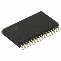
IC PROCESSOR NEURON 32-SOIC
Manufacturer
Cypress Semiconductor Corp
Series
Neuron®r
Datasheet
1.CY7C53120E2-10SXIT.pdf
(14 pages)
Specifications of CY7C53120E2-10SXIT
Applications
Network Processor
Core Processor
Pipelined
Program Memory Type
FLASH (2 kB), ROM (10 kB)
Controller Series
CY7C531xx
Ram Size
2K x 8
Interface
Serial
Number Of I /o
11
Voltage - Supply
4.5 V ~ 5.5 V
Operating Temperature
-40°C ~ 85°C
Mounting Type
Surface Mount
Package / Case
32-SOIC (11.30mm Width)
Lead Free Status / RoHS Status
Lead free / RoHS Compliant


Document #: 38-10001 Rev. *E
External Memory Interface Timing — CY7C53150, V
Differential Transceiver Electrical Characteristics
Notes
15. t
16. Refer to
17. The data hold parameter, t
18. Refer to
19. The three-state condition is when the device is not actively driving data. Refer to
20. To meet the timing above for 20-MHz operation, the loading on A0–A15, D0–D7, and R/W is 30 pF. Loading on E is 20 pF.
21. Common mode voltage is defined as the average value of the waveform at each input at the time switching occurs.
22. Z
t
PW
PW
t
t
t
t
t
t
t
t
t
t
t
t
t
Receiver Common Mode Voltage Range to maintain hysteresis
Receiver Common Mode Range to operate with unspecified hysteresis
Input Offset Voltage
Propagation Delay (F = 0, V
Input Resistance
Wake-up Time
Differential Output Impedance for CP2 and CP3
cyc
AD
AH
RD
RH
WR
WH
DSR
DHR
DHW
DDW
DHZ
DDZ
acc
Parameter
cyc
EH
EL
0
= |V[CP2]-V[CP3] |/40 mA for 4.75 < V
= 2(1/f), where f is the input clock (CLK1) frequency (20, 10, 5, 2.5, 1.25, or 0.625 MHz).
Figure 3
Figure 6
Memory Cycle Time (System Clock Period)
Pulse Width, E High
Pulse Width, E Low
Delay, E High to Address Valid
Address Hold Time After E High
Delay, E High to R/W Valid Read
R/W Hold Time Read After E High
Delay, E High to R/W Valid Write
R/W Hold Time Write After E High
Read Data Setup Time to E High
Data Hold Time Read After E High
Data Hold Time Write After E High
Delay, E Low to Data Valid
Data Three State Hold Time After E Low
Delay, E High to Data Three-State
External Memory Access Time (t
20-MHz input clock
for detailed measurement information.
and
Figure 5
Figure 2. Signal Loading for Timing Specifications Unless Otherwise Specified
DHW
, is measured to the disable levels shown in
for detailed measurement information.
ID
Characteristic
= V
TEST SIGNAL
Figure 3. Test Point Levels for E Pulse Width Measurements
hys
[16]
DD
[16]
/2 + 200 mV)
< 5.25V.
Description
PW
EH
2.0V
[20]
[20]
C
acc
[22]
[20]
L
[18]
[17, 18]
= t
cyc
[19]
– t
[15]
C
C
C
AD
L
L
L
Figure
= 20 pF for E
= 30 pF for A0–A15, D0–D7, and R/W
= 50 pF for all other signals
– t
[21]
0.8V
DSR
Figure 2
DD
5, rather than to the traditional data invalid levels.
) at
± 10%
and
Figure 5
2.0V
PW
–0.05V
(V
EL
DD
Min.
t
t
for detailed measurement information.
1.2
0.9
cyc
cyc
—
—
5
hys
= 4.5V to 5.5 V, T
Min.
100
10
15
10
50
/2 – 5
/2 – 5
—
—
—
—
—
5
5
0
0
– 35
0.05V
V
A
V
t
t
DD
230 ns
cyc
cyc
DD
= –40°C to+ 85°C
Max.
Max.
3200
CY7C53150
CY7C53120
10
35
—
– 1.75
hys
/2 + 5
/2 + 5
35
—
25
—
25
—
—
—
—
12
—
42
—
– 2.2
+ 35
Page 8 of 14
Unit
Unit
MΩ
mV
ns
μs
ns
ns
ns
ns
ns
ns
ns
ns
ns
ns
ns
ns
ns
ns
ns
ns
Ω
V
V
[2]
)
[+] Feedback
Related parts for CY7C53120E2-10SXIT
Image
Part Number
Description
Manufacturer
Datasheet
Request
R

Part Number:
Description:
IC PROCESSOR NEURON 32-SOIC
Manufacturer:
Cypress Semiconductor Corp
Datasheet:

Part Number:
Description:
IC PROCESSOR NEURON 44LQFP
Manufacturer:
Cypress Semiconductor Corp
Datasheet:
Part Number:
Description:
Manufacturer:
Cypress Semiconductor Corp
Datasheet:
Part Number:
Description:
Manufacturer:
Cypress Semiconductor Corp
Datasheet:
Part Number:
Description:
IC PROCESSOR NEURON 44LQFP
Manufacturer:
Cypress Semiconductor Corp
Datasheet:
Part Number:
Description:
Manufacturer:
Cypress Semiconductor Corp
Datasheet:
Part Number:
Description:
Manufacturer:
Cypress Semiconductor Corp
Datasheet:
Part Number:
Description:
Manufacturer:
Cypress Semiconductor Corp
Datasheet: