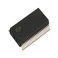
CY8C20566-24PVXIT Cypress Semiconductor Corp, CY8C20566-24PVXIT Datasheet - Page 23

CY8C20566-24PVXIT
Manufacturer Part Number
CY8C20566-24PVXIT
Description
IC MCU 32K FLASH 2K SRAM 48SSOP
Manufacturer
Cypress Semiconductor Corp
Series
CapSense® Controllersr
Specifications of CY8C20566-24PVXIT
Applications
Capacitive Sensing
Core Processor
M8C
Program Memory Type
FLASH (32 kB)
Controller Series
CY8C20xx6
Ram Size
2K x 8
Interface
I²C, SPI
Number Of I /o
36
Voltage - Supply
1.71 V ~ 5.5 V
Operating Temperature
-40°C ~ 85°C
Mounting Type
Surface Mount
Package / Case
48-SSOP
Operating Temperature (min)
-40C
Operating Temperature (max)
85C
Technology
CMOS
Processing Unit
Microprocessor
Operating Supply Voltage (min)
1.71V
Operating Supply Voltage (typ)
1.8/2.5/3.3/5V
Operating Supply Voltage (max)
5.5V
Package Type
SSOP
Screening Level
Industrial
Pin Count
48
Mounting
Surface Mount
Rad Hardened
No
Processor Series
CY8C20x66
Core
M8C
Data Bus Width
8 bit
Program Memory Size
32 KB
Data Ram Size
2 KB
Interface Type
I2C, SPI, USB
Maximum Clock Frequency
24 MHz
Number Of Programmable I/os
36
Number Of Timers
3
Maximum Operating Temperature
+ 85 C
Mounting Style
SMD/SMT
Development Tools By Supplier
CY3280-20X66
Minimum Operating Temperature
- 40 C
Lead Free Status / RoHS Status
Lead free / RoHS Compliant
Lead Free Status / RoHS Status
Compliant, Lead free / RoHS Compliant
Table 25.AC Characteristics – USB Data Timings
Table 26.AC Characteristics – USB Driver
AC Comparator Specifications
The following table lists guaranteed maximum and minimum specifications for the entire voltage and temperature ranges.
Table 27. AC Low Power Comparator Specifications
AC Analog Mux Bus Specifications
The following table lists guaranteed maximum and minimum specifications for the entire voltage and temperature ranges.
Table 28. AC Analog Mux Bus Specifications
Document Number: 001-12696 Rev. *D
Tdrate
Tdjr1
Tdjr2
Tudj1
Tudj2
Tfdeop
Tfeopt
Tfeopr
Tfst
Tr
Tf
TR
Vcrs
T
F
LPC
SW
Symbol
Symbol
Symbol
Symbol
Transition rise time
Transition fall time
Rise/fall time matching
Output signal crossover voltage
Comparator Response Time, 50
mV Overdrive
Switch Rate
Full speed data rate
Receiver data jitter tolerance
Receiver data jitter tolerance
Driver differential jitter
Driver differential jitter
Source jitter for differential
transition
Source SE0 interval of EOP
Receiver SE0 interval of EOP
Width of SE0 interval during
differential transition
Description
Description
Description
Description
GPIO Pin
Voltage
Output
90%
10%
Figure 11. GPIO Timing Diagram
Average bit rate
To next transition
To pair transition
To next transition
To pair transition
To SE0 transition
50 pF
50 pF
50 mV overdrive does not include
offset voltage.
Maximum pin voltage when measuring
switch rate is 1.8Vp-p
TRise23
TRise01
TRise23L
TRise01L
Conditions
Conditions
Conditions
Conditions
TFall
TFallL
CY8C20x36/46/66, CY8C20396
12–0.25%
90.00
-18.5
Min
-4.0
-3.5
160
Min
Min
Min
1.3
82
-9
-2
4
4
–
Typ
Typ
Typ
Typ
12
–
–
–
–
–
–
–
–
–
–
–
–
–
12 + 0.25%
111.1
Max
Max
18.5
Max
175
2.0
Max
3.5
4.0
6.3
20
20
100
14
9
5
Page 23 of 34
Units
Units
Units
MHz
Units
MHz
ns
ns
ns
ns
ns
ns
ns
ns
ns
ns
%
V
ns
[+] Feedback


