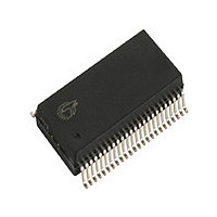
CY8C20566-24PVXIT Cypress Semiconductor Corp, CY8C20566-24PVXIT Datasheet - Page 24

CY8C20566-24PVXIT
Manufacturer Part Number
CY8C20566-24PVXIT
Description
IC MCU 32K FLASH 2K SRAM 48SSOP
Manufacturer
Cypress Semiconductor Corp
Series
CapSense® Controllersr
Specifications of CY8C20566-24PVXIT
Applications
Capacitive Sensing
Core Processor
M8C
Program Memory Type
FLASH (32 kB)
Controller Series
CY8C20xx6
Ram Size
2K x 8
Interface
I²C, SPI
Number Of I /o
36
Voltage - Supply
1.71 V ~ 5.5 V
Operating Temperature
-40°C ~ 85°C
Mounting Type
Surface Mount
Package / Case
48-SSOP
Operating Temperature (min)
-40C
Operating Temperature (max)
85C
Technology
CMOS
Processing Unit
Microprocessor
Operating Supply Voltage (min)
1.71V
Operating Supply Voltage (typ)
1.8/2.5/3.3/5V
Operating Supply Voltage (max)
5.5V
Package Type
SSOP
Screening Level
Industrial
Pin Count
48
Mounting
Surface Mount
Rad Hardened
No
Processor Series
CY8C20x66
Core
M8C
Data Bus Width
8 bit
Program Memory Size
32 KB
Data Ram Size
2 KB
Interface Type
I2C, SPI, USB
Maximum Clock Frequency
24 MHz
Number Of Programmable I/os
36
Number Of Timers
3
Maximum Operating Temperature
+ 85 C
Mounting Style
SMD/SMT
Development Tools By Supplier
CY3280-20X66
Minimum Operating Temperature
- 40 C
Lead Free Status / RoHS Status
Lead free / RoHS Compliant
Lead Free Status / RoHS Status
Compliant, Lead free / RoHS Compliant
AC External Clock Specifications
The following table lists guaranteed maximum and minimum specifications for the entire voltage and temperature ranges.
Table 29. AC External Clock Specifications
AC Programming Specifications
The following table lists the guaranteed maximum and minimum specifications for the entire voltage and temperature ranges.
Table 30. AC Programming Specifications
Document Number: 001-12696 Rev. *D
F
–
–
–
T
T
T
T
F
T
T
T
T
T
Symbol
Symbol
OSCEXT
RSCLK
FSCLK
SSCLK
HSCLK
SCLK
ERASEB
WRITE
DSCLK
DSCLK3
DSCLK2
SCLK (P1[1])
SDATA (P1[0])
Rise Time of SCLK
Fall Time of SCLK
Data Set up Time to Falling Edge of SCLK
Data Hold Time from Falling Edge of SCLK
Frequency of SCLK
Flash Erase Time (Block)
Flash Block Write Time
Data Out Delay from Falling Edge of SCLK 3.6 < Vdd
Data Out Delay from Falling Edge of SCLK 3.0 ≤ Vdd ≤ 3.6
Data Out Delay from Falling Edge of SCLK 1.71 ≤ Vdd ≤ 3.0
Frequency
High Period
Low Period
Power Up IMO to Switch
Description
T
RSCLK
Description
T
SSCLK
T
FSCLK
Figure 12. AC Waveform
T
HSCLK
Conditions
Conditions
CY8C20x36/46/66, CY8C20396
0.750
20.6
20.6
T
Min
150
Min
DSCLK
40
40
1
1
0
–
–
–
–
–
Typ
Typ
–
–
–
–
–
–
–
–
–
–
–
–
–
–
5300
Max
Max
25.2
130
20
20
18
25
60
85
–
–
8
–
–
Page 24 of 34
Units
Units
MHz
MHz
ms
ms
ns
ns
ns
ns
ns
ns
ns
μs
ns
ns
[+] Feedback


