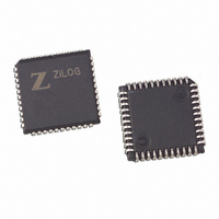
Z85C3008VSG Zilog, Z85C3008VSG Datasheet - Page 41

Z85C3008VSG
Manufacturer Part Number
Z85C3008VSG
Description
IC 8MHZ Z8500 CMOS SCC 44-PLCC
Manufacturer
Zilog
Series
SCCr
Specifications of Z85C3008VSG
Processor Type
Z80
Features
Error Detection and Multiprotocol Support
Speed
8MHz
Voltage
5V
Mounting Type
Surface Mount
Package / Case
44-LCC (J-Lead)
Maximum Operating Temperature
+ 70 C
Minimum Operating Temperature
0 C
Mounting Style
SMD/SMT
Cpu Speed
8MHz
Digital Ic Case Style
LCC
No. Of Pins
44
Supply Voltage Range
5V
Operating Temperature Range
0°C To +70°C
Svhc
No SVHC (18-Jun-2010)
Base Number
85
Rohs Compliant
Yes
Clock Frequency
8MHz
Lead Free Status / RoHS Status
Lead free / RoHS Compliant
Other names
269-3932
Z85C3008VSG
Z85C3008VSG
Available stocks
Company
Part Number
Manufacturer
Quantity
Price
Company:
Part Number:
Z85C3008VSG
Manufacturer:
Zilog
Quantity:
800
Company:
Part Number:
Z85C3008VSG
Manufacturer:
MAX
Quantity:
74
PS011705-0608
INTACK
D7–D0
Z80C30 Timing
RD
Interrupt Acknowledge Cycle Timing
Figure 23
goes Low and the falling edge of RD, the internal and external IEI/IEO daisy chains settle.
If there is an interrupt pending in the SCC and IEI is High when RD falls, the Acknowl-
edge cycle is intended for the SCC. In this case, the SCC can be programmed to respond to
RD Low by placing its interrupt vector on D7-D0. It then sets the appropriate Interrupt-
Under-Service latch internally.
If the external daisy chain is not used, AC parameter #38 is required to settle the interrupt
priority daisy chain internal to the SCC. If the external daisy chain is used, you must
follow the equation in AC Characteristics, Read/Write Timing
for calculating the required daisy-chain settle time.
The SCC generates internal control signals from AS and DS that are related to PCLK.
Because PCLK has no phase relationship with AS and DS, the circuitry generating these
internal control signals must provide time for metastable conditions to disappear. This
gives rise to a recovery time related to PCLK. The recovery time applies only between bus
transactions involving the SCC. The recovery time required for proper operation is speci-
fied from the falling edge of DS in the first transaction involving the SCC to the falling
edge of DS in the second transaction involving the SCC. The timings for Z80C30 device is
described below:
•
•
•
Read Cycle Timing
Write Cycle Timing
Interrupt Acknowledge Cycle Timing
displays an Interrupt Acknowledge cycle timing. Between the time INTACK
Figure 23. Interrupt Acknowledge Cycle Timing
CMOS SCC Serial Communications Controller
Vector
Table 6
Product Specification
Functional Description
on page 47, Note 5
37


