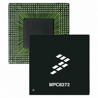
MPC8272CVRMIBA Freescale Semiconductor, MPC8272CVRMIBA Datasheet - Page 25

MPC8272CVRMIBA
Manufacturer Part Number
MPC8272CVRMIBA
Description
IC MPU POWERQUICC II 516-PBGA
Manufacturer
Freescale Semiconductor
Specifications of MPC8272CVRMIBA
Processor Type
MPC82xx PowerQUICC II 32-bit
Speed
266MHz
Voltage
1.5V
Mounting Type
Surface Mount
Package / Case
516-PBGA
Lead Free Status / RoHS Status
Lead free / RoHS Compliant
Features
-
Available stocks
Company
Part Number
Manufacturer
Quantity
Price
Company:
Part Number:
MPC8272CVRMIBA
Manufacturer:
Freescale Semiconductor
Quantity:
135
Company:
Part Number:
MPC8272CVRMIBA
Manufacturer:
Freescale Semiconductor
Quantity:
10 000
Part Number:
MPC8272CVRMIBA
Manufacturer:
N/A
Quantity:
20 000
7
As shown in
Within each mode, the configuration of bus, core, PCI, and CPM frequencies is determined by seven bits
during the power-on reset—three hardware configuration pins (MODCK[1–3]) and four bits from
Freescale Semiconductor
•
•
1
2
JTAG external clock to output high impedance
1
2
3
4
5
6
7
All outputs are measured from the midpoint voltage of the falling/rising edge of t
in question. The output timings are measured at the pins. All output timings assume a purely resistive 50-Ω load.
Time-of-flight delays must be added for trace lengths, vias, and connectors in the system.
The symbols used for timing specifications herein follow the pattern of t
(reference)(state)
t
(V) relative to the t
timing (JT) with respect to the time data input signals (D) went invalid (X) relative to the t
going to the high (H) state. Note that, in general, the clock reference symbol representation is based on three letters
representing the clock of a particular functional. For rise and fall times, the latter convention is used with the
appropriate letter: R (rise) or F (fall).
TRST is an asynchronous level sensitive signal. The setup time is for test purposes only.
Non-JTAG signal input timing with respect to t
Non-JTAG signal output timing with respect to t
Guaranteed by design.
Guaranteed by design and device characterization.
PCI_HOST_EN
Determines PCI clock frequency range.
PCI_CFG[0]
JTDVKH
Clock Configuration Modes
PCI_CFG[0]— An input signal. Also defined as “PCI_HOST_EN.” Refer to the Chapter 6,
“External Signals,” and Chapter 9, “PCI Bridge,” in the MPC8272 PowerQUICC II™ Family
Reference Manual.
PCI_MODCK—Bit 27 in the Hard Reset Configuration Word. Refer to Chapter 5, “Reset,” in the
MPC8272 PowerQUICC II™ Family Reference Manual.
0
0
1
1
Table
symbolizes JTAG device timing (JT) with respect to the time data input signals (D) reaching the valid state
1
for inputs and t(
15, the clocking mode is set according to two sources:
Pins
JTG
Parameter
MPC8272 PowerQUICC II™ Family Hardware Specifications, Rev. 2
PCI_MODCK
clock reference (K) going to the high (H) state or setup time. Also, t
0
1
0
1
(first two letters of functional block)(reference)(state)(signal)(state)
Boundary-scan data
Table 14. JTAG Timings
Table 15. MPC8272 Clocking Modes
2
Clocking Mode
PCI agent
PCI host
TCLK
TDO
TCLK
.
.
Symbol
t
t
JTKLDZ
JTKLOZ
PCI Clock Frequency Range (MHz)
1
2
(continued)
Min
(first two letters of functional block)(signal)(state)
1
1
50–66
25–50
50–66
25–50
TCLK
Max
10
10
for outputs. For example,
to the midpoint of the signal
JTDXKH
JTG
clock reference (K)
Clock Configuration Modes
Unit
ns
ns
symbolizes JTAG
Reference
Table 16
Table 17
Table 18
Table 19
Notes
5
5
,
,
6
6
25


