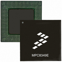
MPC8349VVALFB Freescale Semiconductor, MPC8349VVALFB Datasheet - Page 80

MPC8349VVALFB
Manufacturer Part Number
MPC8349VVALFB
Description
IC MPU POWERQUICC II 672-TBGA
Manufacturer
Freescale Semiconductor
Series
PowerQUICC II PROr
Datasheet
1.MPC8349VVALFB.pdf
(87 pages)
Specifications of MPC8349VVALFB
Processor Type
MPC83xx PowerQUICC II Pro 32-Bit
Speed
667MHz
Voltage
1.3V
Mounting Type
Surface Mount
Package / Case
672-TBGA
Processor Series
MPC8xxx
Core
e300
Data Bus Width
32 bit
Development Tools By Supplier
MPC8349E-MITXE
Maximum Clock Frequency
667 MHz
Maximum Operating Temperature
+ 105 C
Mounting Style
SMD/SMT
I/o Voltage
1.8 V, 2.5 V, 3.3 V
Minimum Operating Temperature
0 C
Family Name
MPC83xx
Device Core
PowerQUICC II Pro
Device Core Size
32b
Frequency (max)
667MHz
Instruction Set Architecture
RISC
Supply Voltage 1 (typ)
1.3V
Operating Supply Voltage (max)
1.36V
Operating Supply Voltage (min)
1.24V
Operating Temp Range
0C to 105C
Operating Temperature Classification
Commercial
Mounting
Surface Mount
Pin Count
672
Package Type
TBGA
Core Size
32 Bit
Program Memory Size
64KB
Cpu Speed
667MHz
Embedded Interface Type
I2C, SPI, USB, UART
Digital Ic Case Style
TBGA
No. Of Pins
672
Rohs Compliant
Yes
For Use With
MPC8349E-MITX-GP - KIT REFERENCE PLATFORM MPC8349EMPC8349E-MITXE - BOARD REFERENCE FOR MPC8349MPC8349EA-MDS-PB - KIT MODULAR DEV SYSTEM MPC8349E
Lead Free Status / RoHS Status
Lead free / RoHS Compliant
Features
-
Lead Free Status / Rohs Status
Lead free / RoHS Compliant
Available stocks
Company
Part Number
Manufacturer
Quantity
Price
Company:
Part Number:
MPC8349VVALFB
Manufacturer:
AD
Quantity:
8 557
Company:
Part Number:
MPC8349VVALFB
Manufacturer:
Freescale Semiconductor
Quantity:
10 000
System Design Information
21.2
Each PLL gets power through independent power supply pins (AV
level should always equal to V
low frequency filter scheme.
There are a number of ways to provide power reliably to the PLLs, but the recommended solution is to
provide four independent filter circuits as illustrated in
Independent filters to each PLL reduce the opportunity to cause noise injection from one PLL to the other.
The circuit filters noise in the PLL resonant frequency range from 500 kHz to 10 MHz. It should be built
with surface mount capacitors with minimum effective series inductance (ESL). Consistent with the
recommendations of Dr. Howard Johnson in High Speed Digital Design: A Handbook of Black Magic
(Prentice Hall, 1993), multiple small capacitors of equal value are recommended over a single large value
capacitor.
To minimize noise coupled from nearby circuits, each circuit should be placed as closely as possible to the
specific AV
pin, which is on the periphery of package, without the inductance of vias.
Figure 41
21.3
Due to large address and data buses and high operating frequencies, the MPC8349EA can generate
transient power surges and high frequency noise in its power supply, especially while driving large
capacitive loads. This noise must be prevented from reaching other components in the MPC8349EA
system, and the device itself requires a clean, tightly regulated source of power. Therefore, the system
designer should place at least one decoupling capacitor at each V
device. These capacitors should receive their power from separate V
power planes in the PCB, with short traces to minimize inductance. Capacitors can be placed directly under
the device using a standard escape pattern. Others can surround the part.
These capacitors should have a value of 0.01 or 0.1 µF. Only ceramic SMT (surface mount technology)
capacitors should be used to minimize lead inductance, preferably 0402 or 0603 sizes.
In addition, distribute several bulk storage capacitors around the PCB, feeding the V
and LV
80
2. The e300 core PLL generates the core clock as a slave to the platform clock. The frequency ratio
DD
between the e300 core clock and the platform clock is selected using the e300 PLL ratio
configuration bits as described in
PLL Power Supply Filtering
Decoupling Recommendations
shows the PLL power supply filter circuit.
planes, to enable quick recharging of the smaller chip capacitors. These bulk capacitors should
MPC8349EA PowerQUICC II Pro Integrated Host Processor Hardware Specifications, Rev. 12
DD
pin being supplied. It should be possible to route directly from the capacitors to the AV
V
DD
DD
Figure 41. PLL Power Supply Filter Circuit
10 Ω
, and preferably these voltages are derived directly from V
2.2 µF
Section 19.2, “Core PLL Configuration.”
GND
Low ESL Surface Mount Capacitors
Figure
2.2 µF
41, one to each of the four AV
DD
DD
, OV
AV
DD
1, AV
DD
, OV
DD
(or L2AV
DD
, GV
DD
2, respectively). The AV
, GV
DD
DD
)
, and LV
DD
Freescale Semiconductor
DD
, LV
, OV
DD
DD
DD
DD
DD
, and GND
pin of the
through a
, GV
pins.
DD
DD
DD
,


