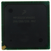
MPC8323CVRADDC Freescale Semiconductor, MPC8323CVRADDC Datasheet - Page 14

MPC8323CVRADDC
Manufacturer Part Number
MPC8323CVRADDC
Description
IC MPU PWRQUICC II 516-PBGA
Manufacturer
Freescale Semiconductor
Datasheet
1.MPC8321VRADDC.pdf
(82 pages)
Specifications of MPC8323CVRADDC
Processor Type
MPC83xx PowerQUICC II Pro 32-Bit
Speed
266MHz
Voltage
1V
Mounting Type
Surface Mount
Package / Case
516-PBGA
For Use With
MPC8323E-RDB - BOARD REFERENCE DESIGN
Lead Free Status / RoHS Status
Lead free / RoHS Compliant
Features
-
Available stocks
Company
Part Number
Manufacturer
Quantity
Price
Company:
Part Number:
MPC8323CVRADDC
Manufacturer:
Freescale Semiconductor
Quantity:
10 000
DDR1 and DDR2 SDRAM
Table 14
MPC8323E when Dn_GV
Table 15
14
Delta input/output capacitance: DQ, DQS
Note:
1. This parameter is sampled. D n
I/O supply voltage
I/O reference voltage
I/O termination voltage
Input high voltage
Input low voltage
Output leakage current
Output high current (V
Output low current (V
Notes:
1. D n
2. MVREF n
3. V
4. Output leakage is measured with all outputs disabled, 0 V
Input/output capacitance: DQ,DQS
Delta input/output capacitance: DQ, DQS
Note:
1. This parameter is sampled. D n
V
Peak-to-peak noise on MVREF n
equal to MVREF n
V
OUT
TT
OUT
MPC8323E PowerQUICC II Pro Integrated Communications Processor Family Hardware Specifications, Rev. 4
_
GV
is not applied directly to the device. It is the supply to which far end signal termination is made and is expected to be
(peak-to-peak) = 0.2 V.
(peak-to-peak) = 0.2 V.
Parameter/Condition
DD
provides the recommended operating conditions for the DDR1 SDRAM component(s) of the
provides the DDR1 capacitance Dn_GV
REF
is expected to be within 50 mV of the DRAM D n
is expected to be equal to 0.5 × D n
Table 14. DDR1 SDRAM DC Electrical Characteristics for D n
Parameter/Condition
Table 15. DDR1 SDRAM Capacitance for D n
REF
OUT
OUT
. This rail should track variations in the DC level of MVREF n
Table 13. DDR2 SDRAM Capacitance for D n
= 0.35 V)
= 1.95 V)
DD
_
_
(typ) = 2.5 V.
GV
REF
GV
DD
DD
may not exceed ±2% of the DC value.
= 1.8 V ± 0.090 V, f = 1 MHz, T
= 2.5 V ± 0.125 V, f = 1 MHz, T
MVREF n
D n
Symbol
_
V
I
V
I
V
I
OZ
OH
OL
GV
TT
IH
IL
_
DD
REF
GV
DD
, and to track D n
MVREF n
MVREF n
DD
Symbol
0.49 × D n
≤
_
C
C
C
(typ) = 2.5 V.
GV
V
DIO
IO
DIO
OUT
DD
2.375
–16.2
–0.3
–9.9
16.2
Min
REF
REF
≤
at all times.
_
D n
GV
_
A
+ 0.15
– 0.04
A
GV
_
= 25 °C, V
_
= 25° C, V
DD
GV
GV
DD
_
Min
—
DD
6
GV
—
DD
(typ) = 2.5 V Interface
.
DC variations as measured at the receiver.
DD
MVREF n
MVREF n
REF
0.51 × D n
OUT
D n
OUT
(typ) = 1.8 V
_
.
_
= D n
GV
GV
= D n
2.625
Max
–9.9
—
—
REF
REF
DD
DD
Max
0.5
_
_
8
_
0.5
GV
(typ) = 2.5 V
GV
+ 0.3
GV
+ 0.04
– 0.15
DD
DD
DD
Freescale Semiconductor
÷ 2,
÷ 2,
Unit
pF
pF
Unit
mA
mA
μA
pF
V
V
V
V
V
Notes
Notes
—
—
—
—
1
1
2
3
4
1
1


