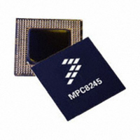
MPC8245TVV300D Freescale Semiconductor, MPC8245TVV300D Datasheet - Page 27

MPC8245TVV300D
Manufacturer Part Number
MPC8245TVV300D
Description
IC MPU 32BIT 300MHZ PPC 352-TBGA
Manufacturer
Freescale Semiconductor
Datasheet
1.MPC8245LZU266D.pdf
(68 pages)
Specifications of MPC8245TVV300D
Processor Type
MPC82xx PowerQUICC II 32-bit
Speed
300MHz
Voltage
1.8V
Mounting Type
Surface Mount
Package / Case
352-TBGA
Processor Series
MPC8xxx
Core
603e
Data Bus Width
32 bit
Maximum Clock Frequency
300 MHz
Operating Supply Voltage
1.8 V, 1.9 V, 2 V, 3.3 V
Maximum Operating Temperature
+ 105 C
Mounting Style
SMD/SMT
Minimum Operating Temperature
- 40 C
Lead Free Status / RoHS Status
Lead free / RoHS Compliant
Features
-
Lead Free Status / Rohs Status
Lead free / RoHS Compliant
Available stocks
Company
Part Number
Manufacturer
Quantity
Price
Company:
Part Number:
MPC8245TVV300D
Manufacturer:
Freescale Semiconductor
Quantity:
135
Company:
Part Number:
MPC8245TVV300D
Manufacturer:
Freescale Semiconductor
Quantity:
10 000
Part Number:
MPC8245TVV300D
Manufacturer:
FREESCALE
Quantity:
20 000
Figure 16
Freescale Semiconductor
All values refer to V
Noise margin at the HIGH level for each connected device (including
hysteresis)
Note:
1. The symbols used for timing specifications follow the pattern of t
2. As a transmitter, the MPC8245 provides a delay time of at least 300 ns for the SDA signal (referred to as the Vihmin of the
3. The maximum t
4. Guaranteed by design.
inputs and t
with respect to the time data input signals (D) reach the valid state (V) relative to the t
(H) state or setup time. Also, t
(S) went invalid (X) relative to the t
timing (I2) for the time that the data with respect to the stop condition (P) reaching the valid state (V) relative to the t
reference (K) going to the high (H) state or setup time. For rise and fall times, the latter convention is used with the appropriate
letter: R (rise) or F (fall).
SCL signal) to bridge the undefined region of the falling edge of SCL to avoid unintended generation of Start or Stop condition.
When the MPC8245acts as the I
and SDA is balanced, the MPC8245 does not cause the unintended generation of a Start or Stop condition. Therefore, the
300 ns SDA output delay time is not a concern. If, under some rare condition, the 300 ns SDA output delay time is required
for the MPC8245 as transmitter, the following setting is recommended for the FDR bit field of the I2CFDR register to ensure
both the desired I
clock frequency is 400 KHz and the digital filter sampling rate register (DFFSR bits in I2CFDR) is programmed with its default
setting of 0x10 (decimal 16):
For details on I
for SCL”.
SDRAM Clock Frequency
FDR Bit Setting
Actual FDR Divider Selected
Actual I
provides the AC test load for the I
(first two letters of functional block)(reference)(state)(signal)(state)
2
C SCL Frequency Generated
IH
2
I2DXKL
C frequency calculation, refer to the application note AN2919 “Determining the I
(min) and V
2
C SCL clock frequency and SDA output delay time are achieved. It is assumed that the desired I
has only to be met if the device does not stretch the LOW period (t
Output
MPC8245 Integrated Processor Hardware Specifications, Rev. 10
Parameter
IL
Table 13. I
(max) levels (see
I2SXKL
2
C bus master while transmitting, it drives both SCL and SDA. As long as the load on SCL
I2C
symbolizes I
clock reference (K) going to the low (L) state or hold time. Also, t
2
C AC Electrical Specifications (continued)
Figure 16. I
Table
260.4 KHz 148.4 KHz
100 MHz
0x00
384
Z
0
= 50 Ω
2
12).
C timing (I2) for the time that the data with respect to the start condition
2
C.
2
133 MHz
0x2A
896
C AC Test Load
(first two letters of functional block)(signal)(state) (reference)(state)
for outputs. For example, t
Symbol
V
NH
R
L
= 50 Ω
1
0.2 × OV
I2C
Min
clock reference (K) going to the high
Electrical and Thermal Characteristics
OV
I2CL
I2DVKH
DD
DD
) of the SCL signal.
/2
2
C Frequency Divider Ratio
symbolizes I
I2PVKH
Max
—
symbolizes I
2
C timing (I2)
I2C
2
C SCL
Unit
clock
V
for
2
C
27


