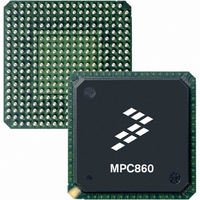
MPC860DPZQ66D4 Freescale Semiconductor, MPC860DPZQ66D4 Datasheet - Page 3

MPC860DPZQ66D4
Manufacturer Part Number
MPC860DPZQ66D4
Description
IC MPU PWRQUICC 66MHZ 357-PBGA
Manufacturer
Freescale Semiconductor
Datasheet
1.MC860DECVR50D4R2.pdf
(80 pages)
Specifications of MPC860DPZQ66D4
Processor Type
MPC8xx PowerQUICC 32-Bit
Speed
66MHz
Voltage
3.3V
Mounting Type
Surface Mount
Package / Case
357-PBGA
Family Name
MPC8xx
Device Core
PowerQUICC
Device Core Size
32b
Frequency (max)
66MHz
Instruction Set Architecture
RISC
Supply Voltage 1 (typ)
2.5/3.3V
Operating Supply Voltage (max)
3.465/3.6V
Operating Supply Voltage (min)
2/3.135V
Operating Temp Range
0C to 95C
Operating Temperature Classification
Commercial
Mounting
Surface Mount
Pin Count
357
Package Type
BGA
Lead Free Status / RoHS Status
Contains lead / RoHS non-compliant
Features
-
Lead Free Status / Rohs Status
Not Compliant
Available stocks
Company
Part Number
Manufacturer
Quantity
Price
Company:
Part Number:
MPC860DPZQ66D4
Manufacturer:
Freescale Semiconductor
Quantity:
10 000
Part Number:
MPC860DPZQ66D4
Manufacturer:
FREESCALE
Quantity:
20 000
2
The following list summarizes the key MPC860 features:
Freescale Semiconductor
•
•
•
•
•
•
Features
Embedded single-issue, 32-bit core (implementing the Power Architecture technology) with
thirty-two 32-bit general-purpose registers (GPRs)
— The core performs branch prediction with conditional prefetch without conditional execution.
— 4- or 8-Kbyte data cache and 4- or 16-Kbyte instruction cache (see
— MMUs with 32-entry TLB, fully-associative instruction, and data TLBs
— MMUs support multiple page sizes of 4-, 16-, and 512-Kbytes, and 8-Mbytes; 16 virtual
— Advanced on-chip-emulation debug mode
Up to 32-bit data bus (dynamic bus sizing for 8, 16, and 32 bits)
32 address lines
Operates at up to 80 MHz
Memory controller (eight banks)
— Contains complete dynamic RAM (DRAM) controller
— Each bank can be a chip select or RAS to support a DRAM bank.
— Up to 15 wait states programmable per memory bank
— Glueless interface to DRAM, SIMMS, SRAM, EPROM, Flash EPROM, and other memory
— DRAM controller programmable to support most size and speed memory interfaces
— Four CAS lines, four WE lines, and one OE line
— Boot chip-select available at reset (options for 8-, 16-, or 32-bit memory)
— Variable block sizes (32 Kbytes to 256 Mbytes)
— Selectable write protection
— On-chip bus arbitration logic
General-purpose timers
— Four 16-bit timers or two 32-bit timers
— Gate mode can enable/disable counting
— Interrupt can be masked on reference match and event capture.
– 16-Kbyte instruction caches are four-way, set-associative with 256 sets; 4-Kbyte instruction
– 8-Kbyte data caches are two-way, set-associative with 256 sets; 4-Kbyte data caches are
– Cache coherency for both instruction and data caches is maintained on 128-bit (4-word)
– Caches are physically addressed, implement a least recently used (LRU) replacement
address spaces and 16 protection groups
devices
caches are two-way, set-associative with 128 sets.
two-way, set-associative with 128 sets.
cache blocks.
algorithm, and are lockable on a cache block basis.
MPC860 PowerQUICC™ Family Hardware Specifications, Rev. 8
Table
1)
Features
3


