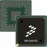
MPC8347EVVAJFB Freescale Semiconductor, MPC8347EVVAJFB Datasheet - Page 16

MPC8347EVVAJFB
Manufacturer Part Number
MPC8347EVVAJFB
Description
IC MPU POWERQUICC II 672-TBGA
Manufacturer
Freescale Semiconductor
Series
PowerQUICC II PROr
Specifications of MPC8347EVVAJFB
Processor Type
MPC83xx PowerQUICC II Pro 32-Bit
Speed
533MHz
Voltage
1.2V
Mounting Type
Surface Mount
Package / Case
672-TBGA
Processor Series
MPC8xxx
Core
e300
Data Bus Width
32 bit
Development Tools By Supplier
MPC8349E-MITXE
Maximum Clock Frequency
533 MHz
Maximum Operating Temperature
+ 105 C
Mounting Style
SMD/SMT
I/o Voltage
1.8 V, 2.5 V, 3.3 V
Minimum Operating Temperature
0 C
Core Size
32 Bit
Program Memory Size
64KB
Cpu Speed
533MHz
Embedded Interface Type
I2C, SPI, USB, UART
Digital Ic Case Style
TBGA
No. Of Pins
672
Rohs Compliant
Yes
Lead Free Status / RoHS Status
Lead free / RoHS Compliant
Features
-
Lead Free Status / Rohs Status
Lead free / RoHS Compliant
Available stocks
Company
Part Number
Manufacturer
Quantity
Price
Company:
Part Number:
MPC8347EVVAJFB
Manufacturer:
Freescale Semiconductor
Quantity:
135
Company:
Part Number:
MPC8347EVVAJFB
Manufacturer:
Freescale Semiconductor
Quantity:
10 000
Part Number:
MPC8347EVVAJFB
Manufacturer:
FREESCALE
Quantity:
20 000
DDR SDRAM
6.2
This section provides the AC electrical characteristics for the DDR SDRAM interface.
6.2.1
Table 13
Figure 4
6.2.2
Table 14
DDR SDRAM interface.
16
At recommended operating conditions with GV
AC input low voltage
AC input high voltage
MDQS—MDQ/MECC input skew per byte
Note:
1. Maximum possible skew between a data strobe (MDQS[n]) and any corresponding bit of data (MDQ[8n + {0...7}] if
0 <= n <= 7) or ECC (MECC[{0...7}] if n = 8).
MDQS[n]
MDQ[x]
illustrates the DDR input timing diagram showing the t
provides the input AC timing specifications for the DDR SDRAM interface.
and
DDR SDRAM AC Electrical Characteristics
MCK[n]
MCK[n]
MPC8347E PowerQUICC™ II Pro Integrated Host Processor Hardware Specifications, Rev. 11
DDR SDRAM Input AC Timing Specifications
DDR SDRAM Output AC Timing Specifications
Table 15
Parameter
provide the output AC timing specifications and measurement conditions for the
Table 13. DDR SDRAM Input AC Timing Specifications
333 MHz
266 MHz
Figure 4.
DD
of 2.5 V ± 5%.
t
t
MCK
DISKEW
DDR Input Timing Diagram
Symbol
t
DISKEW
V
V
IH
IL
D0
MV
REF
Min
—
—
+ 0.31
D1
DISKEW
t
DISKEW
timing parameter.
MV
GV
REF
1125
DD
Max
750
– 0.31
+ 0.3
Freescale Semiconductor
Unit
ps
V
V
Notes
1


