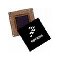
XPC8260ZUHFBC Freescale Semiconductor, XPC8260ZUHFBC Datasheet - Page 17

XPC8260ZUHFBC
Manufacturer Part Number
XPC8260ZUHFBC
Description
IC MPU POWERQUICC II 480-TBGA
Manufacturer
Freescale Semiconductor
Specifications of XPC8260ZUHFBC
Processor Type
MPC82xx PowerQUICC II 32-bit
Speed
166MHz
Voltage
2.5V
Mounting Type
Surface Mount
Package / Case
480-TBGA
Family Name
MPC82XX
Device Core
PowerQUICC II
Device Core Size
32b
Frequency (max)
166MHz
Instruction Set Architecture
RISC
Supply Voltage 1 (typ)
1.8V
Operating Supply Voltage (max)
1.9V
Operating Supply Voltage (min)
1.7V
Operating Temp Range
0C to 105C
Operating Temperature Classification
Commercial
Mounting
Surface Mount
Pin Count
480
Package Type
TBGA
Rohs Compliant
NO
Peak Reflow Compatible (260 C)
No
Lead Free Status / RoHS Status
Contains lead / RoHS non-compliant
Features
-
Lead Free Status / Rohs Status
Not Compliant
Available stocks
Company
Part Number
Manufacturer
Quantity
Price
Company:
Part Number:
XPC8260ZUHFBC
Manufacturer:
HARRIS
Quantity:
6 563
Company:
Part Number:
XPC8260ZUHFBC
Manufacturer:
Freescale Semiconductor
Quantity:
10 000
Part Number:
XPC8260ZUHFBC
Manufacturer:
FREESCALE
Quantity:
20 000
Figure 6
Figure 7
Freescale Semiconductor
MPC8260A PowerQUICC™ II Integrated Communications Processor Hardware Specifications, Rev. 2.0
shows the SCC/SMC/SPI/I
shows TDM input and output signals.
SCC/SMC/SPI/I2C output signals
SCC/SMC/SPI/I2C input signals
(See note.)
(See note.)
Note: There are four possible TDM timing conditions:
1. Input sampled on the rising edge and output driven on the rising edge (shown).
2. Input sampled on the rising edge and output driven on the falling edge.
3. Input sampled on the falling edge and output driven on the falling edge.
4. Input sampled on the falling edge and output driven on the rising edge.
TDM output signals
Note: There are four possible timing conditions for SCC and SPI:
TDM input signals
1. Input sampled on the rising edge and output driven on the rising edge (shown).
2. Input sampled on the rising edge and output driven on the falling edge.
3. Input sampled on the falling edge and output driven on the falling edge.
4. Input sampled on the falling edge and output driven on the rising edge.
Serial CLKin
Figure 6. SCC/SMC/SPI/I
BRG_OUT
2
C internal clock.
Figure 7. TDM Signal Diagram
sp18a
sp20
2
C Internal Clock Diagram
sp40/sp41
sp21
sp19a
sp38a/sp39a
Electrical and Thermal Characteristics
17


