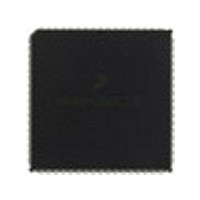
MC68HC000EI12 Freescale Semiconductor, MC68HC000EI12 Datasheet - Page 7

MC68HC000EI12
Manufacturer Part Number
MC68HC000EI12
Description
IC MPU 16BIT 10MHZ 68-PLCC
Manufacturer
Freescale Semiconductor
Specifications of MC68HC000EI12
Processor Type
M680x0 32-Bit
Speed
12MHz
Voltage
3.3V, 5V
Mounting Type
Surface Mount
Package / Case
68-PLCC
Family Name
M68000
Device Core
ColdFire
Device Core Size
16/32Bit
Frequency (max)
12MHz
Instruction Set Architecture
RISC
Supply Voltage 1 (typ)
5V
Operating Supply Voltage (max)
5.25V
Operating Supply Voltage (min)
4.75V
Operating Temp Range
0C to 70C
Operating Temperature Classification
Commercial
Mounting
Surface Mount
Pin Count
68
Package Type
PLCC
Lead Free Status / RoHS Status
Lead free / RoHS Compliant
Features
-
Lead Free Status / Rohs Status
Compliant
Available stocks
Company
Part Number
Manufacturer
Quantity
Price
Company:
Part Number:
MC68HC000EI12
Manufacturer:
FREESCALE
Quantity:
3 400
Company:
Part Number:
MC68HC000EI12
Manufacturer:
INTERSIL
Quantity:
1 980
Company:
Part Number:
MC68HC000EI12
Manufacturer:
Freescale Semiconductor
Quantity:
10 000
Company:
Part Number:
MC68HC000EI12R2
Manufacturer:
FREESCAL
Quantity:
8 831
Number
Figure
2-1
2-2
2-3
2-4
2-5
2-6
2-7
3-1
3-2
3-3
3-4
3-5
4-1
4-2
4-3
4-4
4-5
4-6
5-1
5-2
5-3
5-4
5-5
5-6
5-7
5-8
5-9
5-10
5-11
5-12
5-13
5-14
xii
User Programmer's Model ................................................................................... 2-2
Supervisor Programmer's Model Supplement ..................................................... 2-2
Supervisor Programmer's Model Supplement (MC68010) .................................. 2-3
Status Register .................................................................................................... 2-3
Word Organization In Memory ............................................................................. 2-6
Data Organization In Memory .............................................................................. 2-7
Memory Data Organization (MC68008) ............................................................... 2-3
Input and Output Signals (MC68000, MC68HC000, MC68010) .......................... 3-1
Input and Output Signals ( MC68HC001) ............................................................ 3-2
Input and Output Signals (MC68EC000) ............................................................. 3-2
Input and Output Signals (MC68008 48-Pin Version) .......................................... 3-3
Input and Output Signals (MC68008 52-Pin Version) .......................................... 3-3
Byte Read-Cycle Flowchart.................................................................................. 4-2
Read and Write-Cycle Timing Diagram................................................................ 4-2
Byte Write-Cycle Flowchart .................................................................................. 4-4
Write-Cycle Timing Diagram ................................................................................ 4-4
Read-Modify-Write Cycle Flowchart .................................................................... 4-6
Read-Modify-Write Cycle Timing Diagram........................................................... 4-7
Word Read-Cycle Flowchart ................................................................................ 5-2
Byte Read-Cycle Flowchart.................................................................................. 5-2
Read and Write-Cycle Timing Diagram................................................................ 5-3
Word and Byte Read-Cycle Timing Diagram ....................................................... 5-3
Word Write-Cycle Flowchart ................................................................................ 5-5
Byte Write-Cycle Flowchart .................................................................................. 5-5
Word and Byte Write-Cycle Timing Diagram ....................................................... 5-6
Read-Modify-Write Cycle Flowchart .................................................................... 5-7
Read-Modify-Write Cycle Timing Diagram........................................................... 5-8
CPU Space Address Encoding ............................................................................ 5-9
Interrupt Acknowledge Cycle Timing Diagram ................................................... 5-10
Breakpoint Acknowledge Cycle Timing Diagram ............................................... 5-11
3-Wire Bus Arbitration Flowchart
(NA to 48-Pin MC68008 and MC68EC000 ........................................................ 5-12
2-Wire Bus Arbitration Cycle Flowchart ............................................................. 5-13
LIST OF ILLUSTRATIONS
Freescale Semiconductor, Inc.
For More Information On This Product,
M68000 USER’S MANUAL
Go to: www.freescale.com
Title
MOTOROLA
Number
Page


