MPC8360VVALFH Freescale Semiconductor, MPC8360VVALFH Datasheet - Page 59
MPC8360VVALFH
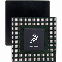
Manufacturer Part Number
MPC8360VVALFH
Description
IC MPU PWRQUICC II 740-TBGA
Manufacturer
Freescale Semiconductor
Datasheet
1.MPC8360CZUAJDG.pdf
(108 pages)
Specifications of MPC8360VVALFH
Processor Type
MPC83xx PowerQUICC II Pro 32-Bit
Speed
667MHz
Voltage
1.3V
Mounting Type
Surface Mount
Package / Case
740-TBGA
For Use With
MPC8360EA-MDS-PB - KIT APPLICATION DEV 8360 SYSTEMMPC8360E-RDK - BOARD REFERENCE DESIGN FOR MPC
Lead Free Status / RoHS Status
Lead free / RoHS Compliant
Features
-
Available stocks
Company
Part Number
Manufacturer
Quantity
Price
Company:

Part Number:
MPC8360VVALFH
Manufacturer:
Freescale Semiconductor
Quantity:
10 000
Company:
Part Number:
MPC8360VVALFHA
Manufacturer:
Freescale Semiconductor
Quantity:
10 000
Part Number:
MPC8360VVALFHA
Manufacturer:
FREESCALE
Quantity:
20 000


16.1
Table 55
16.2
Table 56
Figure 41
Freescale Semiconductor
Output high voltage
Output low voltage
Output low voltage
Input high voltage
Input low voltage
Input current
SPI outputs—Master mode (internal clock) delay
SPI outputs—Slave mode (external clock) delay
SPI inputs—Master mode (internal clock) input setup time
SPI inputs—Master mode (internal clock) input hold time
SPI inputs—Slave mode (external clock) input setup time
SPI inputs—Slave mode (external clock) input hold time
Notes:
1. Output specifications are measured from the 50% level of the rising edge of CLKIN to the 50% level of the signal. Timings
2. The symbols used for timing specifications follow the pattern of t
are measured at the pin.
inputs and t
outputs internal timing (NI) for the time t
valid (V).
MPC8360E/MPC8358E PowerQUICC II Pro Processor Revision 2.x TBGA Silicon Hardware Specifications, Rev. 4
provides the DC electrical characteristics for the device SPI.
and provide the SPI input and output AC timing specifications.
SPI DC Electrical Characteristics
SPI AC Timing Specifications
provides the AC test load for the SPI.
(first two letters of functional block)(reference)(state)(signal)(state)
Characteristic
Output
Characteristic
Table 55. SPI DC Electrical Characteristics
Table 56. SPI AC Timing Specifications
SPI
memory clock reference (K) goes from the high state (H) until outputs (O) are
Figure 41. SPI AC Test Load
Z
0
= 50 Ω
Symbol
V
V
V
V
V
I
OH
OL
IN
OL
IH
IL
0 V ≤ V
(first two letters of functional block)(signal)(state)(reference)(state)
I
for outputs. For example, t
OH
I
I
OL
OL
Condition
= –6.0 mA
= 6.0 mA
= 3.2 mA
IN
—
—
≤ OV
R
Symbol
t
t
L
t
t
t
t
NEKHOX
NEKHOV
t
t
NIKHOX
NIKHOV
NEIVKH
NEIXKH
NIIVKH
NIIXKH
= 50 Ω
DD
2
1
OV
–0.3
Min
2.4
2.0
—
—
—
NIKHOV
DD
Min
0.3
—
—
2
8
0
4
2
/2
symbolizes the NMSI
OV
DD
Max
±10
0.5
0.4
0.8
Max
—
—
—
—
—
—
—
8
8
+ 0.3
Unit
Unit
μA
ns
ns
ns
ns
ns
ns
for
V
V
V
V
V
SPI
59
Related parts for MPC8360VVALFH
Image
Part Number
Description
Manufacturer
Datasheet
Request
R

Part Number:
Description:
Manufacturer:
Freescale Semiconductor, Inc
Datasheet:
Part Number:
Description:
Manufacturer:
Freescale Semiconductor, Inc
Datasheet:
Part Number:
Description:
Manufacturer:
Freescale Semiconductor, Inc
Datasheet:
Part Number:
Description:
Manufacturer:
Freescale Semiconductor, Inc
Datasheet:
Part Number:
Description:
Manufacturer:
Freescale Semiconductor, Inc
Datasheet:
Part Number:
Description:
Manufacturer:
Freescale Semiconductor, Inc
Datasheet:
Part Number:
Description:
Manufacturer:
Freescale Semiconductor, Inc
Datasheet:
Part Number:
Description:
Manufacturer:
Freescale Semiconductor, Inc
Datasheet:
Part Number:
Description:
Manufacturer:
Freescale Semiconductor, Inc
Datasheet:
Part Number:
Description:
Manufacturer:
Freescale Semiconductor, Inc
Datasheet:
Part Number:
Description:
Manufacturer:
Freescale Semiconductor, Inc
Datasheet:
Part Number:
Description:
Manufacturer:
Freescale Semiconductor, Inc
Datasheet:
Part Number:
Description:
Manufacturer:
Freescale Semiconductor, Inc
Datasheet:
Part Number:
Description:
Manufacturer:
Freescale Semiconductor, Inc
Datasheet:
Part Number:
Description:
Manufacturer:
Freescale Semiconductor, Inc
Datasheet: