MPC8313EVRAFFB Freescale Semiconductor, MPC8313EVRAFFB Datasheet - Page 44
MPC8313EVRAFFB
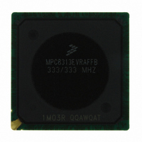
Manufacturer Part Number
MPC8313EVRAFFB
Description
IC MPU POWERQUICC II PRO 516PBGA
Manufacturer
Freescale Semiconductor
Datasheet
1.MPC8313CZQAFFB.pdf
(100 pages)
Specifications of MPC8313EVRAFFB
Processor Type
MPC83xx PowerQUICC II Pro 32-Bit
Speed
333MHz
Voltage
0.95 V ~ 1.05 V
Mounting Type
Surface Mount
Package / Case
516-PBGA
Processor Series
MPC8xxx
Core
e300
Data Bus Width
32 bit
Development Tools By Supplier
MPC8313E-RDB
Maximum Clock Frequency
400 MHz
Operating Supply Voltage
- 0.3 V to + 1.26 V
Maximum Operating Temperature
+ 105 C
Mounting Style
SMD/SMT
Data Ram Size
16 KB
I/o Voltage
2.5 V
Interface Type
I2C, SPI, UART
Minimum Operating Temperature
- 40 C
Program Memory Type
EEPROM/Flash
For Use With
MPC8313E-RDB - BOARD PROCESSOR
Lead Free Status / RoHS Status
Lead free / RoHS Compliant
Features
-
Lead Free Status / Rohs Status
Lead free / RoHS Compliant
Available stocks
Company
Part Number
Manufacturer
Quantity
Price
Company:

Part Number:
MPC8313EVRAFFB
Manufacturer:
FREESCAL
Quantity:
150
Company:
Part Number:
MPC8313EVRAFFB
Manufacturer:
Freescale Semiconductor
Quantity:
10 000


High-Speed Serial Interfaces (HSSI)
The other detailed AC requirements of the SerDes reference clocks is defined by each interface protocol
based on application usage. Refer to the following section for detailed information:
9.2.4.1
SD_REF_CLK/SD_REF_CLK are not intended to be used with, and should not be clocked by, a spread
spectrum clock source.
44
At recommended operating conditions with XV
Rising edge rate (SDn_REF_CLK) to falling edge rate
(SDn_REF_CLK) matching
Notes:
1. Measurement taken from single-ended waveform.
2. Measurement taken from differential waveform.
3. Measured from –200 to +200 mV on the differential waveform (derived from SD n _REF_CLK minus SD n _REF_CLK). The
4. Matching applies to rising edge rate for SD n _REF_CLK and falling edge rate for SD n _REF_CLK. It is measured using a
signal must be monotonic through the measurement region for rise and fall time. The 400 mV measurement window is
centered on the differential zero crossing. See
200 mV window centered on the median cross point, where SD n _REF_CLK rising meets SD n _REF_CLK falling. The median
cross point is used to calculate the voltage thresholds the oscilloscope is to use for the edge rate calculations. The rise edge
rate of SD n _REF_CLK should be compared to the fall edge rate of SD n _REF_CLK, the maximum allowed difference should
not exceed 20% of the slowest edge rate. See
•
SD n _REF_CLK
SD n _REF_CLK
V
V
IH
IL
SD n _REF_CLK
SD n _REF_CLK
SD n _REF_CLK
V
Section 8.3.2, “AC Requirements for SGMII SD_REF_CLK and SD_REF_CLK”
= +200 mV
= –200 mV
CROSS MEDIAN
Minus
0.0 V
Spread Spectrum Clock
Figure 32. Single-Ended Measurement Points for Rise and Fall Time Matching
Table 40. SerDes Reference Clock Common AC Parameters (continued)
MPC8313E PowerQUICC
Figure 31. Differential Measurement Points for Rise and Fall Time
Parameter
Rise Edge Rage
DD_SRDS1
™
Figure
Figure
or XV
II Pro Processor Hardware Specifications, Rev. 3
DD_SRDS2
31.
32.
V
V
CROSS MEDIAN
CROSS MEDIAN
= 1.0 V ± 5%.
matching
Symbol
Rise-fall
SD n _REF_CLK
SD n _REF_CLK
V
CROSS MEDIAN
+ 100 mV
– 100 mV
Min
—
Fall Edge Rate
T
FALL
Max
20
Freescale Semiconductor
T
RISE
Unit
%
Notes
1, 4
Related parts for MPC8313EVRAFFB
Image
Part Number
Description
Manufacturer
Datasheet
Request
R

Part Number:
Description:
Mpc8313e Powerquicc Ii Pro Processor
Manufacturer:
Freescale Semiconductor, Inc
Datasheet:

Part Number:
Description:
BOARD PROCESSOR
Manufacturer:
Freescale Semiconductor
Datasheet:

Part Number:
Description:
BOARD CPU 8313E VER 2.1
Manufacturer:
Freescale Semiconductor
Datasheet:

Part Number:
Description:
BOARD CPU 8313E VER 2.2
Manufacturer:
Freescale Semiconductor
Datasheet:
Part Number:
Description:
Microprocessors - MPU 8313 REV2.2 PB ENC EXT
Manufacturer:
Freescale Semiconductor
Datasheet:
Part Number:
Description:
Microprocessors - MPU 8313 REV2.2 PB W/ENC
Manufacturer:
Freescale Semiconductor
Datasheet:
Part Number:
Description:
Manufacturer:
Freescale Semiconductor, Inc
Datasheet:
Part Number:
Description:
Manufacturer:
Freescale Semiconductor, Inc
Datasheet:
Part Number:
Description:
Manufacturer:
Freescale Semiconductor, Inc
Datasheet:
Part Number:
Description:
Manufacturer:
Freescale Semiconductor, Inc
Datasheet:
Part Number:
Description:
Manufacturer:
Freescale Semiconductor, Inc
Datasheet:
Part Number:
Description:
Manufacturer:
Freescale Semiconductor, Inc
Datasheet:
Part Number:
Description:
Manufacturer:
Freescale Semiconductor, Inc
Datasheet:
Part Number:
Description:
Manufacturer:
Freescale Semiconductor, Inc
Datasheet:
Part Number:
Description:
Manufacturer:
Freescale Semiconductor, Inc
Datasheet: