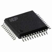
UDA1384H/N1,557 NXP Semiconductors, UDA1384H/N1,557 Datasheet - Page 18

UDA1384H/N1,557
Manufacturer Part Number
UDA1384H/N1,557
Description
IC AUDIO CODEC 44-QFP
Manufacturer
NXP Semiconductors
Type
Audio Codecr
Datasheet
1.UDA1384HN1557.pdf
(55 pages)
Specifications of UDA1384H/N1,557
Data Interface
I²C, Serial
Resolution (bits)
24 b
Number Of Adcs / Dacs
5 / 6
Sigma Delta
No
S/n Ratio, Adcs / Dacs (db) Typ
98 / 110 (Differential), 98 / 110 (Single-Ended)
Voltage - Supply, Analog
2.7 V ~ 3.6 V
Voltage - Supply, Digital
2.7 V ~ 3.6 V
Operating Temperature
-20°C ~ 85°C
Mounting Type
Surface Mount
Package / Case
44-MQFP, 44-PQFP
Lead Free Status / RoHS Status
Lead free / RoHS Compliant
Other names
568-3450
935274756557
UDA1384H
935274756557
UDA1384H
Available stocks
Company
Part Number
Manufacturer
Quantity
Price
Company:
Part Number:
UDA1384H/N1,557
Manufacturer:
NXP Semiconductors
Quantity:
10 000
Philips Semiconductors
9397 750 14366
Product data sheet
9.4 Data write mode
9.5 Data read mode
The data write mode is explained in the signal diagram of
device, 4 bytes must be sent (see
It should be noted that each time a new destination register address needs to be written,
the device address must be sent again.
Table 14:
To read data from the device, a prepare read must first be done and then data read. The
data read mode is explained in the signal diagram of
For reading data from a device, the following 6 bytes are involved (see
Byte
1
2
3
4
1. Byte 1 starting with ‘01’ for signalling the write action to the device, followed by the
2. Byte 2 starting with a ‘0’ for signalling the write action, followed by 7 bits indicating the
3. Byte 3 with bit D15 being the MSB
4. Byte 4 with bit D0 being the LSB
1. Byte 1 with the device address, including ‘01’ for signalling the write action to the
2. Byte 2 is sent with the register address from which data needs to be read. This byte
3. Byte 3 with the device address, including ‘11’ is sent to the device. The ‘11’ indicates
4. Byte 4 sent by the device to the bus, with the (requested) register address and a flag
5. Byte 5 sent by the device to the bus, with the data information in binary format, with
6. Byte 6 sent by the device to the bus, with the data information in binary format, with
device address ‘01 0100’
destination address in binary format with bit A6 being the MSB and bit A0 being the
LSB
device.
starts with a ‘1’, which indicates that there will be a read action from the register,
followed by 7 bits for the destination address in binary format, with bit A6 being the
MSB and bit A0 being the LSB.
that the device must write data to the microcontroller.
bit indicating whether the requested register was valid (bit is logic 0) or invalid (bit is
logic 1).
bit D15 being the MSB.
bit D0 being the LSB.
L3-bus
mode
address
data
transfer
data
transfer
data
transfer
L3-bus write data
Action
device
address
register
address
data
byte 1
data
byte 2
Rev. 02 — 17 January 2005
First in time
Bit 0
0
0
D15
D7
Table
Bit 1
1
A6
D14
D6
14):
Bit 2
0
A5
D13
D5
Bit 3
1
A4
D12
D4
Multichannel audio coder-decoder
Figure
Figure
Bit 4
0
A3
D11
D3
© Koninklijke Philips Electronics N.V. 2005. All rights reserved.
12.
11. For writing data to a
Bit 5
1
A2
D10
D2
UDA1384
Table
Latest in time
Bit 6
0
A1
D9
D1
15):
Bit 7
0
A0
D8
D0
18 of 55


