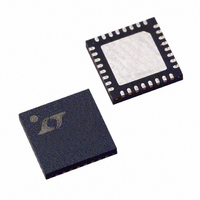
LTC1955EUH Linear Technology, LTC1955EUH Datasheet - Page 7

LTC1955EUH
Manufacturer Part Number
LTC1955EUH
Description
IC INTERFACE DL SMART CARD 32QFN
Manufacturer
Linear Technology
Datasheet
1.LTC1955EUHPBF.pdf
(20 pages)
Specifications of LTC1955EUH
Controller Type
Smart Card Interface
Interface
4-Wire Serial
Voltage - Supply
1.7 V ~ 5.5 V
Current - Supply
10µA
Operating Temperature
-40°C ~ 85°C
Mounting Type
Surface Mount
Package / Case
32-QFN
Lead Free Status / RoHS Status
Contains lead / RoHS non-compliant
Available stocks
Company
Part Number
Manufacturer
Quantity
Price
Company:
Part Number:
LTC1955EUH
Manufacturer:
LT
Quantity:
10 000
Part Number:
LTC1955EUH
Manufacturer:
LINEAR/凌特
Quantity:
20 000
Company:
Part Number:
LTC1955EUH#PBF
Manufacturer:
ADI
Quantity:
5
Part Number:
LTC1955EUH#PBF
Manufacturer:
LINEAR/凌特
Quantity:
20 000
Part Number:
LTC1955EUH#TRPBF
Manufacturer:
LINEAR/凌特
Quantity:
20 000
PIN FUNCTIONS
SCLK: Input. The SCLK pin clocks the serial port. Each
new data bit is received on the rising edge of SCLK. SCLK
should be left high during idle times and should not be
clocked when LD is low.
LD: Input. The falling edge of this pin loads the current
state of the shift register into the command register.
Command changes to both smart card channels will be
updated on the falling edge of LD. The rising edge of LD
latches status information from the smart card channels
into the shift register for the next read/write cycle.
NC/NO: Input. This pin controls the activation level of the
PRES A/PRES B pins. When it is high (DV
pins are active high. When it is low (GND), the PRES pins
are active low. When a ground side N.O. switch is used,
the NC/NO pin should be grounded. When a ground side
N.C. switch is used, the NC/NO pin should be connected
to DV
Note: If an N.C. switch is used, a small current (several
microamperes) will fl ow through the switch whenever a
smart card is not present. For ultralow power consumption
in shutdown, an N.O. switch is optimum.
PRES A/PRES B: Card Socket. The PRES A/PRES B pins
are used to detect the presence of the smart cards. They
can be connected to either normally open or normally
closed detection switches on the smart card acceptor’s
sockets. The NC/NO pin should be set appropriately. These
pins have a pull-up current source on-chip so no external
components are required.
C4A/C8A: Card Socket. These pins connect to the C4
and C8 pins of synchronous memory cards on smart
card socket A. The signal for these pins is unidirectional
and can only be sent to the card. Data for C4A and C8A
is transmitted via the DATA pin and may be selected
in place of I/OA via the serial port (see Table 4). When
either C4A or C8A is selected, it will follow the DATA
pin. When it is deselected, it will remain latched at its
current state.
CC
.
CC
), the PRES
I/O A/I/O B: Card Socket. The I/O A/I/O B pins connect to
the I/O pins of the respective smart card sockets. When
a smart card is selected, its I/O pin connects to the DATA
pin. When a smart card is deselected, its I/O A/I/O B pin
returns to the idle state (H).
RST A/RST B: Card Socket. These pins should be connected
to the RST pins of the respective smart card sockets. The
RST A/RST B signals are derived from the R
a card is selected, its RST pin follows R
is deselected, the RST A/RST B pin for that channel holds
the current value on R
CLK A/CLK B: Card Socket. The CLK A/CLK B pins should
be connected to the CLK pins of the respective smart card
sockets. The CLK A/CLK B signals can be derived from
either the SYNC input or the ASYNC input depending on
which type of card is being accessed. The card type is
selected via the serial port (see Tables 1 and 3).
V
connected to the V
sockets. The activation of a V
the serial port (see Tables 1 and 2) and can be set to 0V,
1.8V, 3V or 5V. The voltage levels of the two card sockets
are controlled independently for maximum fl exibility.
FAULT: Output. The FAULT pin can be used as an interrupt
to a microcontroller to indicate when a fault has occurred.
It is an open-drain output, which is logically equivalent to
D4 + D5 + D12 + D13. (See Table 1)
UNDERV: Input. The UNDERV pin provides security by
supplying a precision undervoltage threshold for ex-
ternal supply monitoring. An external resistive voltage
divider programs the desired undervoltage threshold.
Once UNDERV falls below 1.23V, the LTC1955 automati-
cally begins the deactivation sequence on any channel
that is active.
If external supply monitoring is not required, the UNDERV
pin should be connected to either SV
CCA
, V
CCB
: Card Socket. The V
CC
IN
pins of the respective smart card
.
CCA
/V
CCA
CCB
/V
BATT
CCB
pin is controlled by
LTC1955
IN
pins should be
or DV
. When a card
IN
pin. When
CC
.
1955fb
7


