VNC1L-1A-REEL FTDI, Future Technology Devices International Ltd, VNC1L-1A-REEL Datasheet - Page 16
VNC1L-1A-REEL
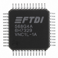
Manufacturer Part Number
VNC1L-1A-REEL
Description
IC USB HOST CTLR VINCULUM 48LQFP
Manufacturer
FTDI, Future Technology Devices International Ltd
Series
Vinculumr
Datasheet
1.VNC1L-1A-REEL.pdf
(32 pages)
Specifications of VNC1L-1A-REEL
Controller Type
USB 2.0 Controller
Interface
SPI
Voltage - Supply
3 V ~ 3.6 V
Current - Supply
25mA
Operating Temperature
0°C ~ 70°C
Mounting Type
Surface Mount
Package / Case
48-LQFP
For Use With
768-1006 - BOARD DEV FOR VINCULUM VNC1L-1A768-1005 - MOD USB FLASH DISK FILE TRANSFER768-1002 - MOD MCU-USB HOST CTLR 40-DIP768-1001 - MOD MCU-USB HOST CTLR 24-DIP27937 - MEMORY STICK DATALOGGER
Lead Free Status / RoHS Status
Lead free / RoHS Compliant
Other names
768-1000-2
Available stocks
Company
Part Number
Manufacturer
Quantity
Price
Company:

Part Number:
VNC1L-1A-REEL
Manufacturer:
TI
Quantity:
3 485
Part Number:
VNC1L-1A-REEL
Manufacturer:
FTDI
Quantity:
20 000


5.2 SPI Interface
When the data and control buses are configured in SPI mode, the interface operates as an SPI Slave. An
SPI master is required to provide the clock (SCLK) signal and set the chip select (CS) for the duration of
the transaction. The SPI interface is a polled 4-wire interface which can operate at speeds up to 12MHz
The SPI interface differs from most other implementations in that it uses a 13 clock sequence to transfer
a single byte of data. In addition to a „Start‟ state, the SPI master must send two setup bits which
indicate data direction and target address. The encoding of the setup bits is shown in Table 5.3. A single
data byte is transmitted in each SPI transaction, with the most significant bit transmitted first.
After each transaction VNC1L returns a single status bit. This indicates if a Data Write was successful or a
Data Read was valid.
Table 5.3 SPI Setup Bit Encoding
5.2.1 Signal Descriptions
Table 5.4 Data and Control Bus Signal Mode Options - SPI Interface
The VNC1L SPI interface uses 4 signal lines: SCLK, CS, SDI and SDO. The signals SDI, SDO and CS
are always clocked on the rising edge of the SCLK signal.
CS signal must be raised high for the duration of the entire transaction. For data transactions, the CS
must be released for at least one clock cycle after a transaction has completed. It is not necessary to
release CS between Status Read operations.
The „Start‟ state of SDI and CS high on the rising edge of SCLK initiates the transfer. The transfer finishes
after 13 clock cycles, and the next transfer starts when SDI is high during the rising edge of SCLK.
The following Figure 5.3 and Table 5.5 give details of the bus timing requirements.
Pin No.
31
32
33
34
Direction
(R/W)
1
1
0
0
Name
SCLK
SDO
SDI
CS
Copyright © 2009 Future Technology Devices International Limited
Address
Target
0
1
0
1
Output
Input
Input
Input
Type
Vinculum VNC1L Embedded USB Host Controller IC Datasheet Version 2.02
Description
SPI Clock input
SPI Serial Data Input
SPI Serial Data Output
SPI Chip Select Input
Operation
Data Read
Status Read
Data Write
N/A
Meaning
Retrieve byte from Transmit Buffer
Read SPI Interface Status
Add byte to Receive Buffer
N/A
Document Reference No.: FT_000030
Clearance No.: FTDI# 50
16
Related parts for VNC1L-1A-REEL
Image
Part Number
Description
Manufacturer
Datasheet
Request
R

Part Number:
Description:
Vinculum Vnc1l Embedded Usb Host Controller Ic
Manufacturer:
Future Technology Devices International Ltd.
Datasheet:

Part Number:
Description:
IC, USB HOST CONTROLLER, LQFP-48
Manufacturer:
FTDI
Datasheet:
Part Number:
Description:
USB Interface IC USB Vinculum Host /Dev Ctrl IC LQFP-48
Manufacturer:
FTDI
Datasheet:

Part Number:
Description:
IC USB TO SERIAL UART 32-QFN
Manufacturer:
FTDI, Future Technology Devices International Ltd

Part Number:
Description:
IC USB HOST VINCULUM-II 32QFN
Manufacturer:
FTDI, Future Technology Devices International Ltd
Datasheet:
Part Number:
Description:
IC USB HOST VINCULUM-II 32LQFN
Manufacturer:
FTDI, Future Technology Devices International Ltd
Datasheet:
Part Number:
Description:
IC USB HOST VINCULUM-II 48QFN
Manufacturer:
FTDI, Future Technology Devices International Ltd
Datasheet:
Part Number:
Description:
IC USB HOST VINCULUM-II 32LQFN
Manufacturer:
FTDI, Future Technology Devices International Ltd
Datasheet:
Part Number:
Description:
IC USB HOST VINCULUM-II 32QFN
Manufacturer:
FTDI, Future Technology Devices International Ltd
Datasheet:
Part Number:
Description:
IC USB HOST VINCULUM-II 48LQFP
Manufacturer:
FTDI, Future Technology Devices International Ltd
Datasheet:
Part Number:
Description:
IC USB HOST VINCULUM-II 48LQFP
Manufacturer:
FTDI, Future Technology Devices International Ltd
Datasheet:
Part Number:
Description:
IC USB HOST VINCULUM-II 48QFN
Manufacturer:
FTDI, Future Technology Devices International Ltd
Datasheet:
Part Number:
Description:
IC USB HOST CTLR VINCULUM 64QFN
Manufacturer:
FTDI, Future Technology Devices International Ltd
Datasheet:

Part Number:
Description:
IC USB HOST CTLR VINCULUM 64LQFP
Manufacturer:
FTDI, Future Technology Devices International Ltd
Datasheet:
Part Number:
Description:
IC USB HOST VINCULUM-II 64LQFP
Manufacturer:
FTDI, Future Technology Devices International Ltd
Datasheet: